Status of Flex circuit, VLDB and Hybrid Mauro Citterio ——-On
19 Slides2.35 MB
Status of Flex circuit, VLDB and Hybrid Mauro Citterio -------On behalf of the INFN Team: Alessandro Andreani Nadim Conti Nicola Neri Marco Petruzzo Fabrizio Sabatini 5/18/2016 Mauro Citterio - UT Milano Workshop 1
Index First generation flex cable Summary Lesson learned Second generation flex cable Flex PCB design: four layer flex a rigid stiffener Results/observations Lesson Learned MegArray to VLDB Adapter Hybrid 5/18/2016 Flex circuit design: four layer flex Layout description Optimization Hybrid schedule: prototype production Mauro Citterio - UT Milano Workshop 22
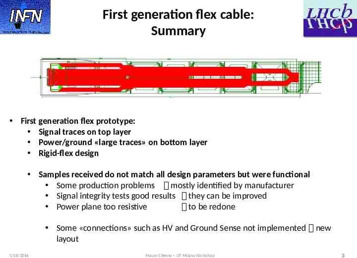
First generation flex cable: Summary First generation flex prototype: Signal traces on top layer Power/ground «large traces» on bottom layer Rigid-flex design Samples received do not match all design parameters but were functional Some production problems mostly identified by manufacturer Signal integrity tests good results they can be improved Power plane too resistive to be redone Some «connections» such as HV and Ground Sense not implemented new layout 5/18/2016 Mauro Citterio - UT Milano Workshop 33
First generation flex cable: Lesson Learned Layout needed optimization Improved in 2nd generation design Electrical parameter tuned Production issues Manufacturer requested adjustments 50% of samples showed broken or semi-open traces Visual inspection indicated poor process quality Prototype production: very long time About 6 months to have samples Production was not done on a “production line” No feedback on what result to expect in a new production Adopted strategy 5/18/2016 Produce a new set of cable with CERN PCB shop Prototypes yes, production “maybe” New design & new technical files Keep technical files “generic” to have large potential manufacturer market for full production Mauro Citterio - UT Milano Workshop 44
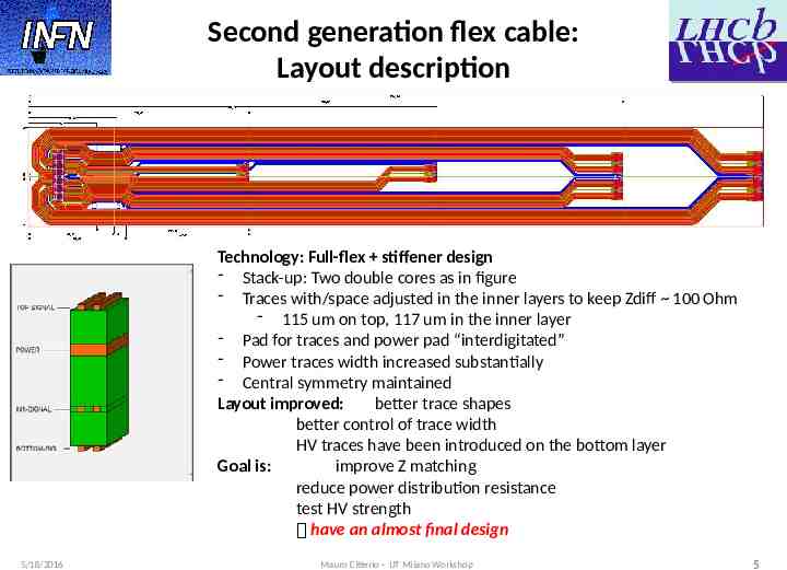
Second generation flex cable: Layout description Technology: Full-flex stiffener design - Stack-up: Two double cores as in figure - Traces with/space adjusted in the inner layers to keep Zdiff 100 Ohm - 115 um on top, 117 um in the inner layer - Pad for traces and power pad “interdigitated” - Power traces width increased substantially - Central symmetry maintained Layout improved: better trace shapes better control of trace width HV traces have been introduced on the bottom layer Goal is: improve Z matching reduce power distribution resistance test HV strength have an almost final design 5/18/2016 Mauro Citterio - UT Milano Workshop 55
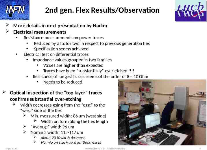
2nd gen. Flex Results/Observation More details in next presentation by Nadim Electrical measurements Resistance measurements on power traces Reduced by a factor two in respect to previous generation flex Specification seems achieved Electrical test on differential traces Impedance values grouped in two families Values are higher than expected Traces have been “substantially” over-etched !!!! Resistance of longest traces seems of the order of 8 – 10 Ohm Needs to be reduced Optical inspection of the “top layer” traces confirms substantial over-etching Width decreases going from the “east” to the “west” side of the flex Min. measured width: 86 um (west side) Width uniform along the flex length “Average” width 96 um Nominal width: 115-117 um 5/18/2016 about 20 % width decrease No info on stack-up layer thicknesses Mauro Citterio - UT Milano Workshop 6
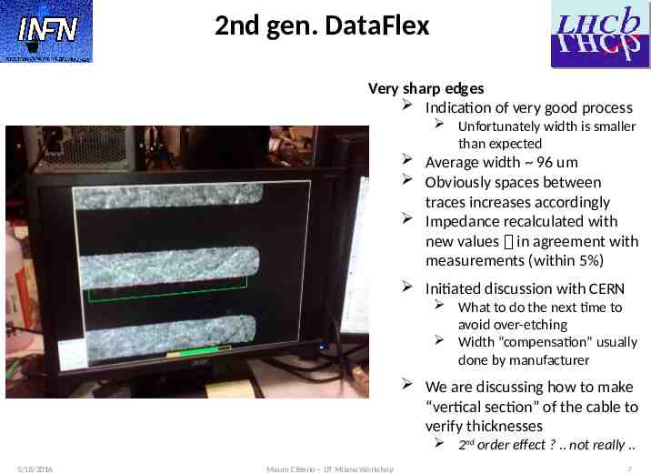
2nd gen. DataFlex Very sharp edges Indication of very good process Unfortunately width is smaller than expected Average width 96 um Obviously spaces between traces increases accordingly Impedance recalculated with new values in agreement with measurements (within 5%) Initiated discussion with CERN What to do the next time to avoid over-etching Width “compensation” usually done by manufacturer We are discussing how to make “vertical section” of the cable to verify thicknesses 2nd order effect ? . not really . 5/18/2016 Mauro Citterio - UT Milano Workshop 7
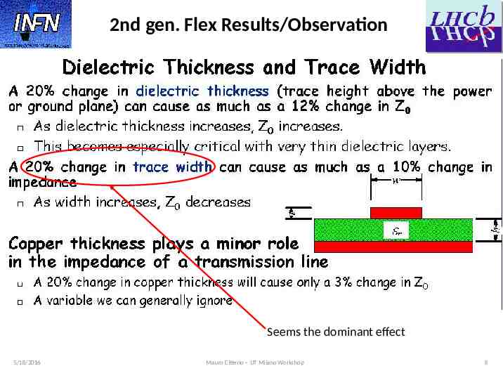
2nd gen. Flex Results/Observation Seems the dominant effect 5/18/2016 Mauro Citterio - UT Milano Workshop 8
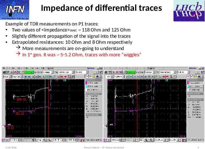
Impedance of differential traces Example of TDR measurements on P1 traces: Meas urem Two values of impedance ave: 118 Ohm and 125 Ohm ents d i n iscuss next p Slightly different propagation of the signal into the traces ed r esent Extrapolated resistances: 10 Ohm and 8 Ohm respectively ation More measurements are on-going to understand In 1st gen. R was 5-5.2 Ohm, traces with more “wiggles” 100 W 50 W 0W 5/18/2016 Mauro Citterio - UT Milano Workshop 9
2nd generation flex cable: Lesson Learned Design shows good progresses toward final version Improved in in respect to 1st generation Most of the electrical parameter tuned Production results Technical issue: over-etching Production done in two steps First two samples with minor problems ( 2.5 months) Eight “good” samples delivered ( 3 months later) Visual inspection indicated very high process quality Prototype production: very long time still !! About 6 months to have samples as before Each sample was “nursed” by loving hands Proposed strategy for next step Complete tests in Milan/Syracuse/Maryland Draft a summary of results end of May Make a list of “actions” to be implemented (hopefully few) Finalize design with strict contact with vendor (Altaflex and eventually a second vendor) 5/18/2016 Design updated by Syracuse meeting, discussed and approved by mid-July CERN technical files match ALTAFLEX production lines Altaflex suggestions: produce few samples to tailor the process order in July, samples back in 3-4 weeks REDO impedance calculation with POLAR (it will be done at Altaflex) Mauro Citterio - UT Milano Workshop 10 10
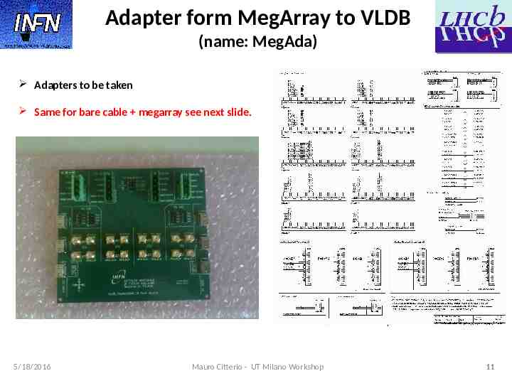
Adapter form MegArray to VLDB (name: MegAda) Adapters to be taken Same for bare cable megarray see next slide. 5/18/2016 Mauro Citterio - UT Milano Workshop 11
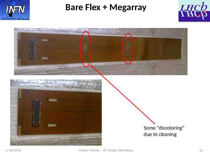
Bare Flex Megarray Some “discoloring” due to cleaning 5/18/2016 Mauro Citterio - UT Milano Workshop 12
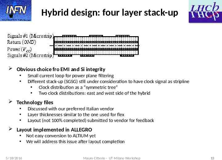
Hybrid design: four layer stack-up Obvious choice fro EMI and Si integrity Small current loop for power plane filtering Different stack-up (SGSG) still under consideration to have clock signal as stripline Clock distribution as a “symmetric tree” Two clock distributions: east and west side of the hybrid Technology files Discussed with our preferred Italian vendor Layer thicknesses similar to the one used for flex Layout (not 100% completed) submitted to vendor for feedback Layout implemented in ALLEGRO 5/18/2016 Not easy conversion to ALTIUM yet We will address this issue after layout completion Mauro Citterio - UT Milano Workshop 13
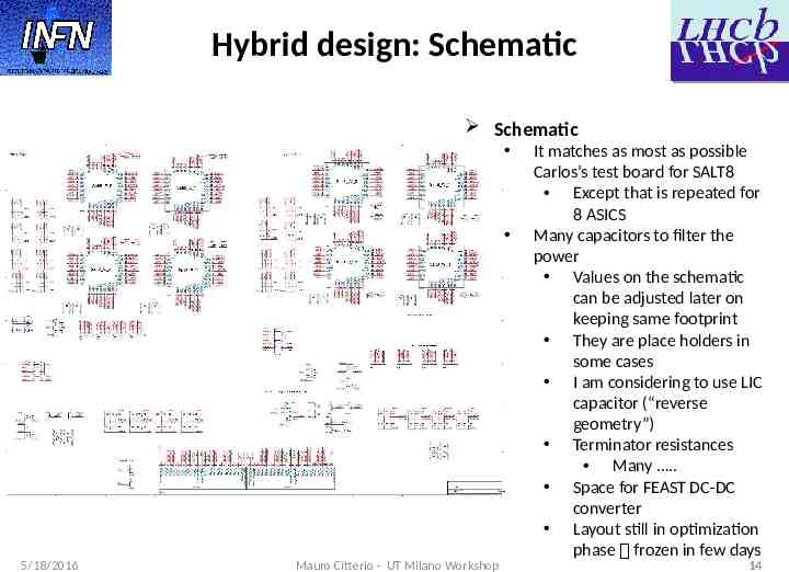
Hybrid design: Schematic Schematic 5/18/2016 Mauro Citterio - UT Milano Workshop It matches as most as possible Carlos’s test board for SALT8 Except that is repeated for 8 ASICS Many capacitors to filter the power Values on the schematic can be adjusted later on keeping same footprint They are place holders in some cases I am considering to use LIC capacitor (“reverse geometry”) Terminator resistances Many . Space for FEAST DC-DC converter Layout still in optimization phase frozen in few days 14
Hybrid design: four layer stack-up Obvious choice fro EMI and Si integrity Small current loop for power plane filtering Different stack-up (SGSG) still under consideration to have clock signal as stripline Clock distribution as a “symmetric tree” Two clock distributions: east and west side of the hybrid Technology files Discussed with our preferred Italian vendor Layer thicknesses similar to the one used for flex Layout (not 100% completed) submitted to vendor for feedback Layout implemented in ALLEGRO 5/18/2016 Not easy conversion to ALTIUM yet We will address this issue after layout completion Mauro Citterio - UT Milano Workshop 15
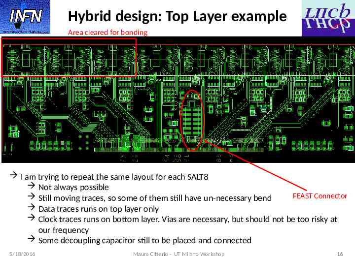
Hybrid design: Top Layer example Area cleared for bonding I am trying to repeat the same layout for each SALT8 Not always possible FEAST Connector Still moving traces, so some of them still have un-necessary bend Data traces runs on top layer only Clock traces runs on bottom layer. Vias are necessary, but should not be too risky at our frequency Some decoupling capacitor still to be placed and connected 5/18/2016 Mauro Citterio - UT Milano Workshop 16
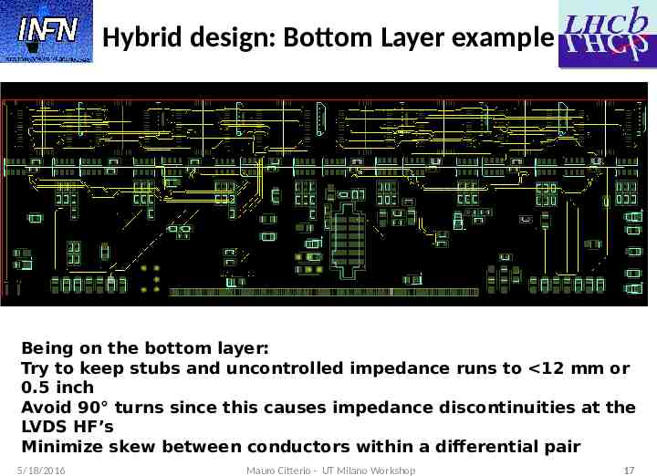
Hybrid design: Bottom Layer example Being on the bottom layer: Try to keep stubs and uncontrolled impedance runs to 12 mm or 0.5 inch Avoid 90 turns since this causes impedance discontinuities at the LVDS HF’s Minimize skew between conductors within a differential pair 5/18/2016 Mauro Citterio - UT Milano Workshop 17
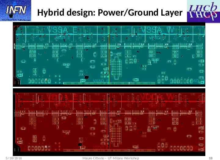
Hybrid design: Power/Ground Layer 5/18/2016 Mauro Citterio - UT Milano Workshop 18
Hybrid Schedule Plan is to finish layout by end of the week Few days for comments Expected turn around not less than 3-4 weeks (Italian vendor) production 12 w-days assembly 2-3 w-days Hybrid available for ASICs bonding mid June Altaflex venue . 5/18/2016 Still to be investigated The layout as of today is “enough” to get a feedback Mauro Citterio - UT Milano Workshop 19
