PSP Family of Compact Models Overview and Recent Developments MOS-AK
43 Slides3.06 MB
PSP Family of Compact Models Overview and Recent Developments MOS-AK December 13th, 2008 G. Gildenblat, W. Wu, X. Li, Z. Zhu, W. Yao, Q. Zhou, G. Dessai, and A. Dey G.D.J. Smit, A.J. Scholten, and D.B.M. Klaassen 1
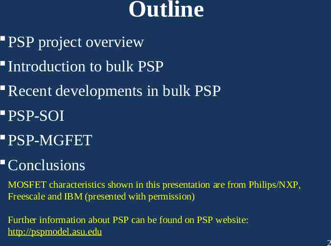
Outline PSP project overview Introduction to bulk PSP Recent developments in bulk PSP PSP-SOI PSP-MGFET Conclusions MOSFET characteristics shown in this presentation are from Philips/NXP, Freescale and IBM (presented with permission) Further information about PSP can be found on PSP website: http://pspmodel.asu.edu 2
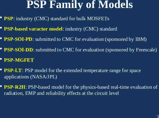
PSP Family of Models PSP: industry (CMC) standard for bulk MOSFETs PSP-based varactor model: industry (CMC) standard PSP-SOI-PD: submitted to CMC for evaluation (sponsored by IBM) PSP-SOI-DD: submitted to CMC for evaluation (sponsored by Freescale) PSP-MGFET PSP-LT: PSP model for the extended temperature range for space applications (NASA/JPL) PSP-R2H: PSP-based model for the physics-based real-time evaluation of radiation, EMP and reliability effects at the circuit level 3
Outline PSP project overview Introduction to bulk PSP Recent developments in bulk PSP PSP-SOI PSP-MGFET Conclusions 4
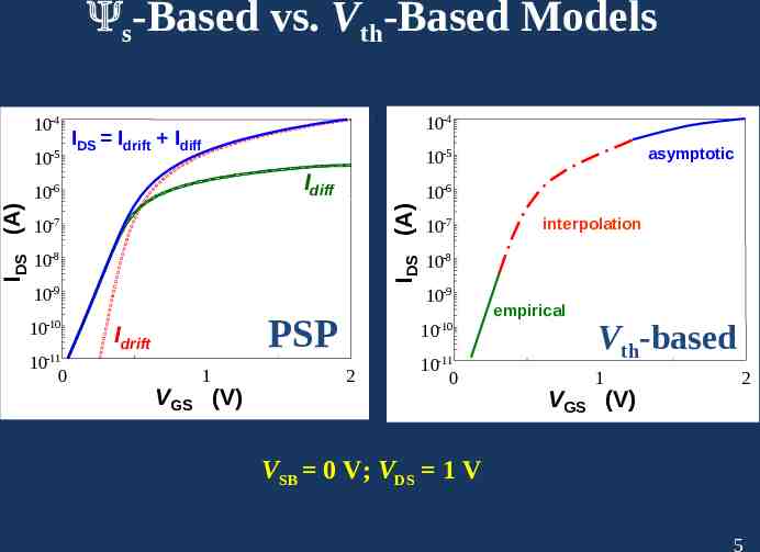
s-Based vs. Vth-Based Models 10-4 -5 10 10-4 IDS Idrift Idiff Idiff 10-6 IDS (A) IDS (A) 10-6 10-7 10-8 10-9 -10 10 10-11 0 asymptotic 10-5 10-7 10-8 10-9 PSP Idrift 1 VGS (V) -10 10 2 interpolation 10-11 0 empirical Vth-based 1 VGS (V) 2 VSB 0 V; VDS 1 V 5
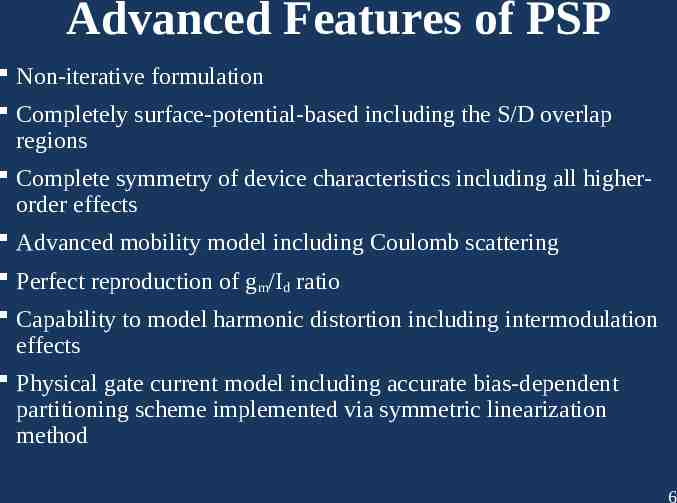
Advanced Features of PSP Non-iterative formulation Completely surface-potential-based including the S/D overlap regions Complete symmetry of device characteristics including all higherorder effects Advanced mobility model including Coulomb scattering Perfect reproduction of gm/Id ratio Capability to model harmonic distortion including intermodulation effects Physical gate current model including accurate bias-dependent partitioning scheme implemented via symmetric linearization method 6
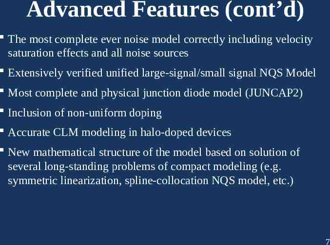
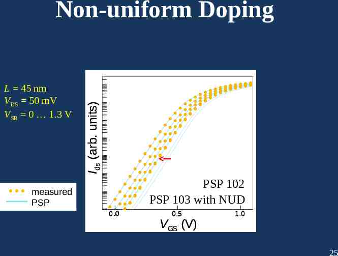
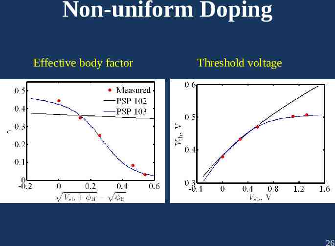
Advanced Features (cont’d) The most complete ever noise model correctly including velocity saturation effects and all noise sources Extensively verified unified large-signal/small signal NQS Model Most complete and physical junction diode model (JUNCAP2) Inclusion of non-uniform doping Accurate CLM modeling in halo-doped devices New mathematical structure of the model based on solution of several long-standing problems of compact modeling (e.g. symmetric linearization, spline-collocation NQS model, etc.) 7
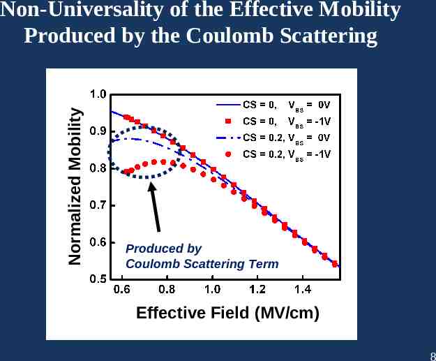
Normalized Mobility Non-Universality of the Effective Mobility Produced by the Coulomb Scattering Produced by Coulomb Scattering Term Effective Field (MV/cm) 8
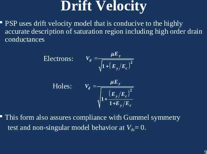
Drift Velocity PSP uses drift velocity model that is conducive to the highly accurate description of saturation region including high order drain conductances Electrons: Ey Vd 1 E y Ec Holes: 2 Ey Vd 1 E y Ec 2 1 E y Ec This form also assures compliance with Gummel symmetry test and non-singular model behavior at Vds 0. 9
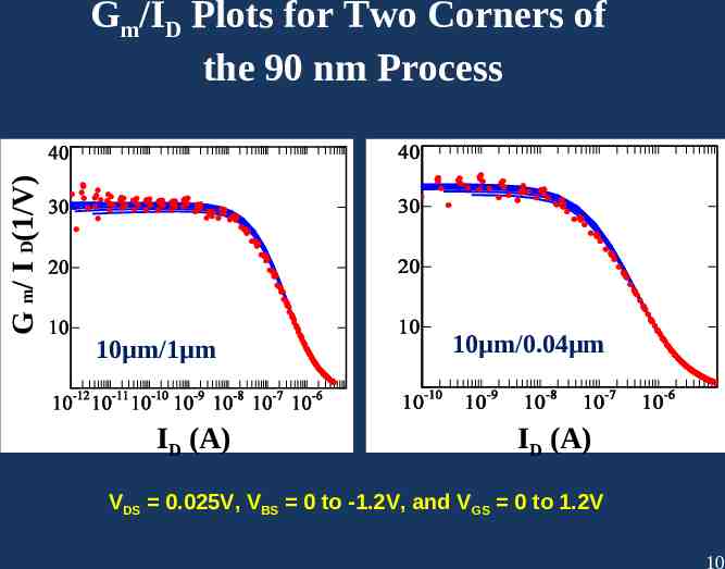
G m/ I D(1/V) Gm/ID Plots for Two Corners of the 90 nm Process 10µm/1µm ID (A) 10µm/0.04µm ID (A) VDS 0.025V, VBS 0 to -1.2V, and VGS 0 to 1.2V 10
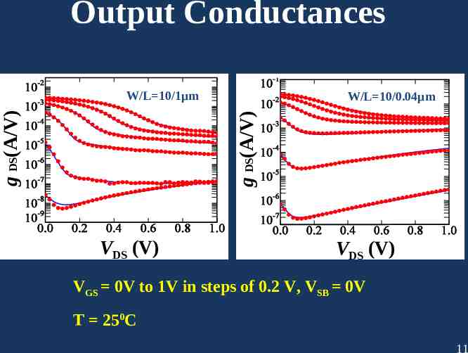
Output Conductances W/L 10/0.04µm g DS(A/V) g DS(A/V) W/L 10/1µm VDS (V) VDS (V) VGS 0V to 1V in steps of 0.2 V, VSB 0V T 250C 11
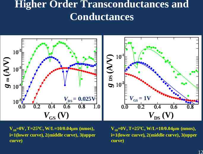
g m (A/V) i g DS (A/V) i Higher Order Transconductances and Conductances VDS 0.025V VGS (V) VSB 0V, T 250C, W/L 10/0.04µm (nmos), i 1(lower curve), 2(middle curve), 3(upper curve) VGS 1V VDS (V) VSB 0V, T 250C, W/L 10/0.04µm (nmos), i 1(lower curve), 2(middle curve), 3(upper curve) 12
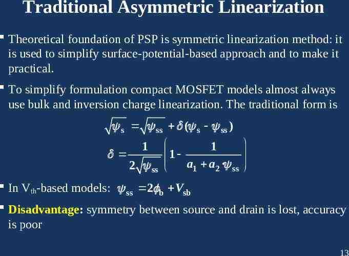
Traditional Asymmetric Linearization Theoretical foundation of PSP is symmetric linearization method: it is used to simplify surface-potential-based approach and to make it practical. To simplify formulation compact MOSFET models almost always use bulk and inversion charge linearization. The traditional form is s ss ( s ss ) 1 2 ss 1 1 a1 a2 · ss In Vth-based models: ss 2 b Vsb Disadvantage: symmetry between source and drain is lost, accuracy is poor 13
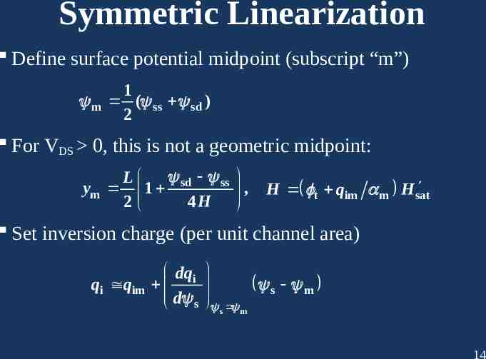
Symmetric Linearization Define surface potential midpoint (subscript “m”) m 1 ( ss sd ) 2 For VDS 0, this is not a geometric midpoint: L sd ss ym 1 2 4H , H t qim m H sat Set inversion charge (per unit channel area) qi qim dqi s m d s s m 14
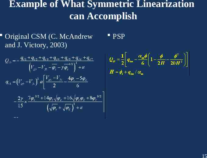
Example of What Symmetric Linearization can Accomplish Original CSM (C. McAndrew and J. Victory, 2003) PSP 15
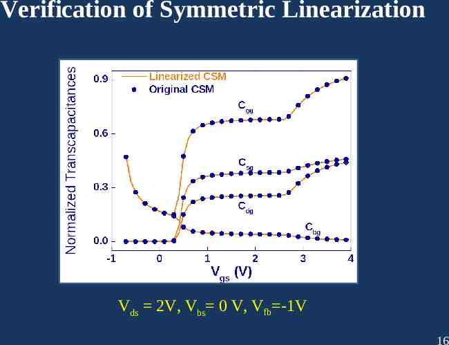
Verification of Symmetric Linearization Vds 2V, Vbs 0 V, Vfb -1V 16
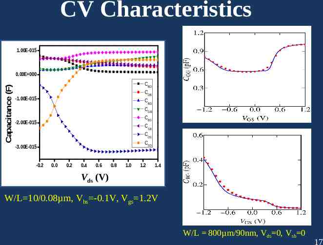
CV Characteristics 1.00E-015 Capacitance (F) 0.00E 000 CBD CDB -1.00E-015 CBG CGB CBS -2.00E-015 CSB CDS CSD -3.00E-015 -0.2 0.0 0.2 0.4 0.6 0.8 1.0 1.2 1.4 (V) VdsVd(V) W/L 10/0.08µm, Vbs -0.1V, Vgs 1.2V W/L 800µm/90nm, Vds 0, Vsb 0 17
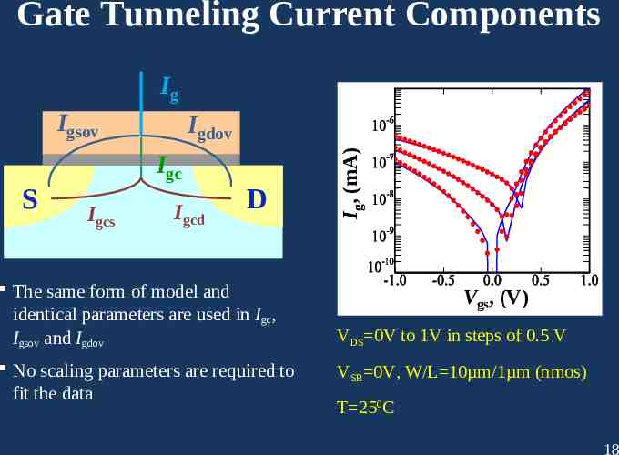
Gate Tunneling Current Components Ig Igsov Igc Igcs Igcd D The same form of model and identical parameters are used in Igc, Igsov and Igdov No scaling parameters are required to fit the data Ig, (mA) S Igdov Vgs, (V) VDS 0V to 1V in steps of 0.5 V VSB 0V, W/L 10µm/1µm (nmos) T 250C 18
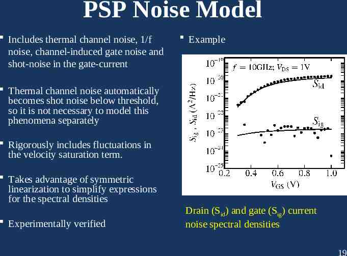
PSP Noise Model Includes thermal channel noise, 1/f noise, channel-induced gate noise and shot-noise in the gate-current Example Thermal channel noise automatically becomes shot noise below threshold, so it is not necessary to model this phenomena separately Rigorously includes fluctuations in the velocity saturation term. Takes advantage of symmetric linearization to simplify expressions for the spectral densities Experimentally verified Drain (Sid) and gate (Sig) current noise spectral densities 19
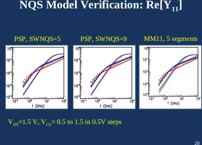
NQS Model Verification: Re[Y11] PSP, SWNQS 5 PSP, SWNQS 9 MM11, 5 segments VDS 1.5 V, VGS 0.5 to 1.5 in 0.5V steps 20
Outline PSP project overview Introduction to bulk PSP Recent developments in bulk PSP PSP-SOI PSP-MGFET Conclusions 21
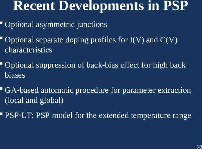
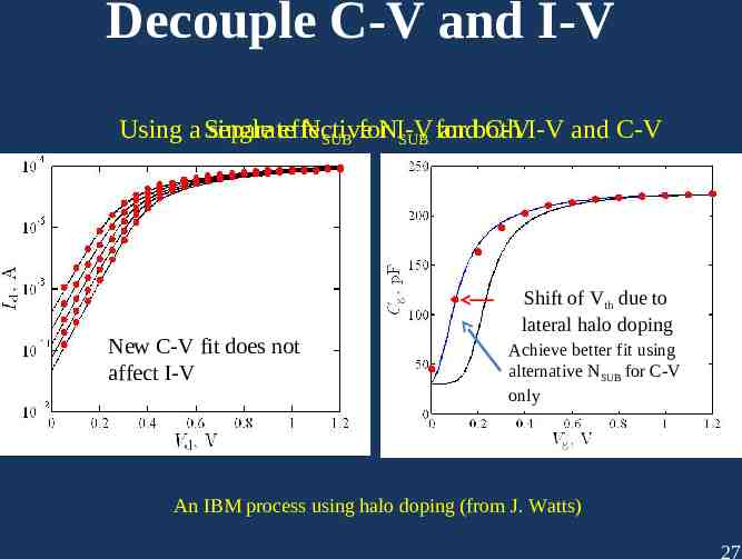
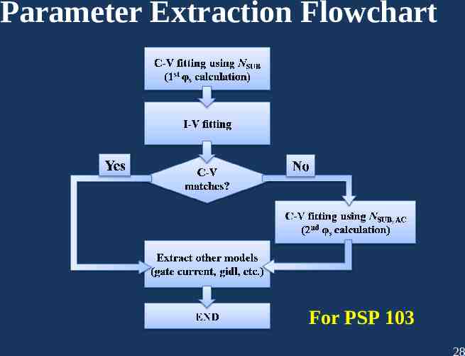
Recent Developments in PSP Optional asymmetric junctions Optional separate doping profiles for I(V) and C(V) characteristics Optional suppression of back-bias effect for high back biases GA-based automatic procedure for parameter extraction (local and global) PSP-LT: PSP model for the extended temperature range 22
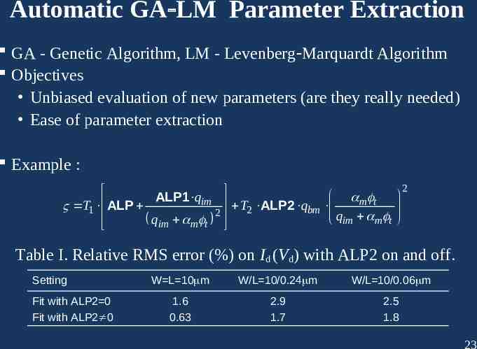
Automatic GA LM Parameter Extraction GA - Genetic Algorithm, LM - Levenberg Marquardt Algorithm Objectives Unbiased evaluation of new parameters (are they really needed) Ease of parameter extraction Example : m t ALP1 qim T2 ALP2 qbm T1 ALP 2 q qim m t im m t 2 Table I. Relative RMS error (%) on Id (Vd) with ALP2 on and off. Setting Fit with ALP2 0 Fit with ALP2 0 W L 10 m W/L 10/0.24 m W/L 10/0.06 m 1.6 0.63 2.9 1.7 2.5 1.8 23
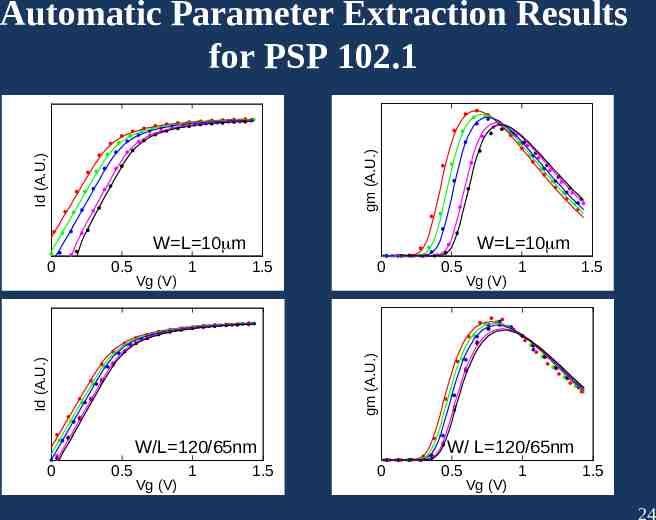
Id (A.U.) gm (A.U.) Automatic Parameter Extraction Results for PSP 102.1 W L 10 m Vg (V) 1 1.5 0 W/L 120/65nm 0 0.5 Vg (V) 1 1.5 gm (A.U.) 0.5 Id (A.U.) 0 W L 10 m 0.5 Vg (V) 1 1.5 W/ L 120/65nm 0 0.5 Vg (V) 1 1.5 24
L 45 nm VDS 50 mV VSB 0 1.3 V Ids (arb. units) Non-uniform Doping PSP 102 PSP 103 with NUD measured PSP 0.0 0.5 VGS (V) 1.0 25
Non-uniform Doping Effective body factor Threshold voltage 26
Decouple C-V and I-V Using a Separate single effective NSUB forNI-V andboth C-VI-V and C-V SUB for New C-V fit does not affect I-V Shift of Vth due to lateral halo doping Achieve better fit using alternative NSUB for C-V only An IBM process using halo doping (from J. Watts) 27
Parameter Extraction Flowchart For PSP 103 28
Outline PSP project overview Introduction to bulk PSP Recent development in bulk PSP PSP-SOI PSP-MGFET Conclusions 29
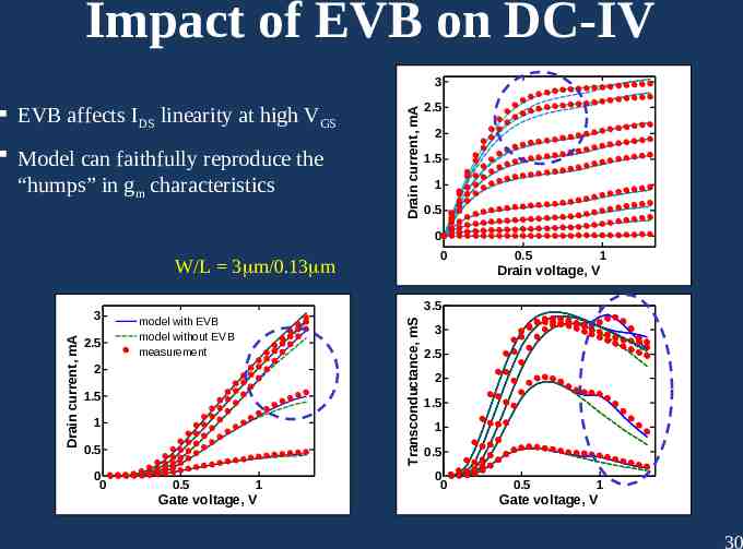
Impact of EVB on DC-IV EVB affects IDS linearity at high VGS Model can faithfully reproduce the “humps” in gm characteristics Drain current, mA 3 2.5 2 1.5 1 0.5 0 0 W/L 3 m/0.13 m 2.5 model with EVB model without EVB measurement 2 1.5 1 0.5 0 0 1 0.5 1 3.5 Transconductance, mS Drain current, mA 3 0.5 Drain voltage, V 0.5 1 Gate voltage, V 3 2.5 2 1.5 1 0.5 0 0 Gate voltage, V 30
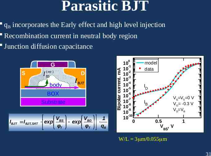
Parasitic BJT qB incorporates the Early effect and high level injection Recombination current in neutral body region Junction diffusion capacitance G S ( rec ) I BS D I BJT body BOX Substrate I BJT I BJT, SAT V exp BS φT V 1 exp BD φT qB Bipolar current. mA 0 10 -1 10 -2 10 -3 10 -4 10 -5 10 -6 10 -7 10 -8 10 -9 10 -10 10 0 model data ID VE VS 0 V VG -0.3 V VD VB IB 0.5 V ,V 1 BS W/L 3 m/0.055 m 31
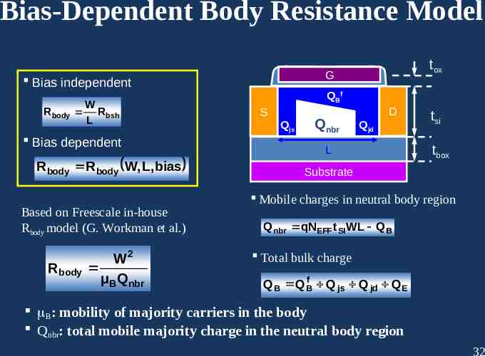
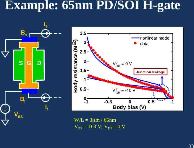
Bias-Dependent Body Resistance Model G Bias independent R body W R bsh L Bias dependent R body R body W, L, bias Based on Freescale in-house Rbody model (G. Workman et al.) R body W2 μB Q nbr tox QBf S Qjs Qnbr D Qjd L tsi tbox Substrate Mobile charges in neutral body region Q nbr qNEFF t SI WL Q B Total bulk charge Q B Q Bf Q js Q jd Q E B: mobility of majority carriers in the body Qnbr: total mobile majority charge in the neutral body region 32
Example: 65nm PD/SOI H-gate IS Bs Body resistance (M ) 3.5 S G D - Bf If VBS nonlinear model data 3 2.5 2 VbGB 0 V 1.5 Junction leakage 1 0.5 0 -1 VbGB -10 V -0.5 0 Body bias (V) 0.5 1 W/L 3 m / 65nm VGS -0.3 V; VDS 0 V 33
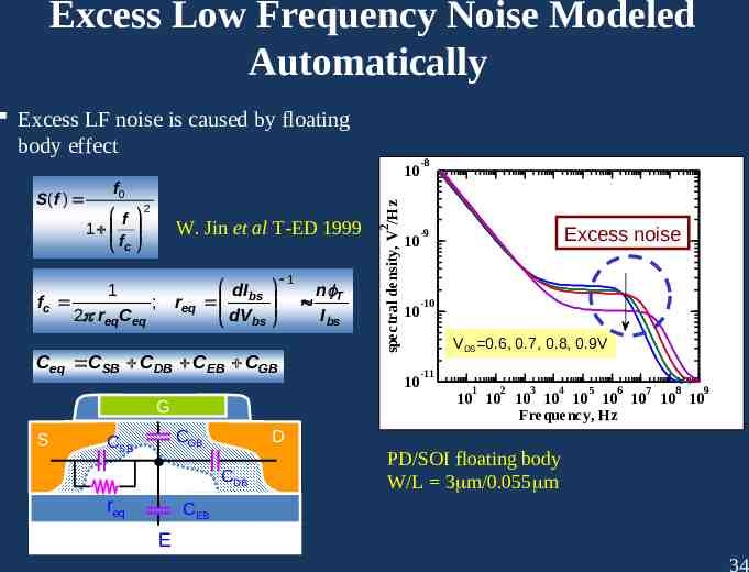
Excess Low Frequency Noise Modeled Automatically Excess LF noise is caused by floating body effect f0 f 1 fc fc 2 1 2 req Ceq W. Jin et al T-ED 1999 ; req dI bs dVbs 1 Ceq CSB CDB CEB CGB G S Drain noise voltage 2 spectral density, V /Hz S (f ) 10 CGB CSB n T I bs 10 Excess noise -9 -10 VDS 0.6, 0.7, 0.8, 0.9V 10 -11 1 2 3 4 5 6 7 8 10 10 10 10 10 10 10 10 10 Frequency, Hz 9 D CDB req 10 -8 PD/SOI floating body W/L 3 m/0.055 m CEB E 34
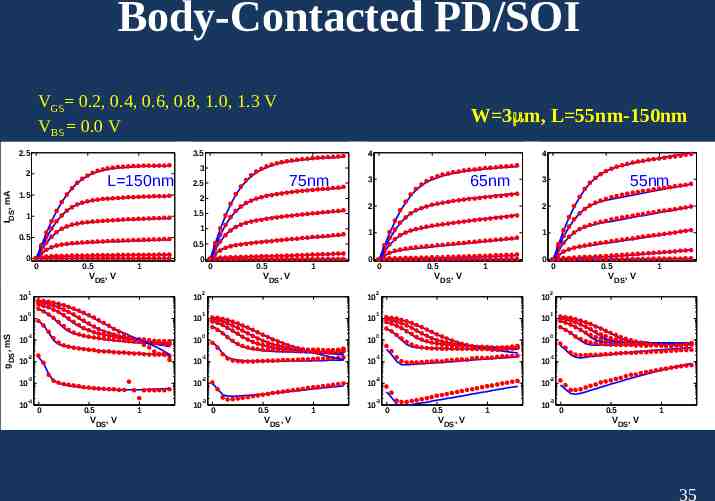
Body-Contacted PD/SOI VGS 0.2, 0.4, 0.6, 0.8, 1.0, 1.3 V VBS 0.0 V 3.5 3 L 150nm 1 65nm 2 55nm 3 1 2 1 0.5 VDS, V 0 1 10 1 10 10 0 10 10 -1 10 -2 10 -3 10 -4 0 0.5 VDS, V 10 1 10 0 10 -1 10 -2 VDS, V 1 10 0.5 VDS, V 10 1 10 VDS, V 1 VDS, V 1 1 0 10 -1 10 10 0.5 2 0 10 -1 10 -2 10 -3 0.5 0 2 -2 0 0 1 10 -3 0.5 0 2 10 0 0 1 gDS, mS 0.5 gDS, mS 0 gDS, mS gDS, mS 1.5 1 0.5 0 2 4 3 IDS, mA 1.5 75nm 2.5 IDS, mA IDS, mA 2 4 IDS, mA 2.5 W 3 m, L 55nm-150nm -3 0 0.5 VDS, V 1 10 0 0.5 VDS, V 1 35
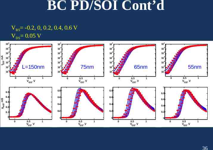
BC PD/SOI Cont’d 0 10 10 -1 10 10 -2 10 10 -3 10 -4 10 -5 10 -6 10 -1 10 -2 10 -3 10 -4 10 75nm -5 10 -6 IDS, mA L 150nm 0 0.5 VGS, V 1 10 -1 10 -2 10 -1 -2 -3 10 -4 10 65nm -5 10 -6 10 0 0 0 IDS, mA 10 IDS, mA IDS, mA VBS -0.2, 0, 0.2, 0.4, 0.6 V VDS 0.05 V 0.5 VGS, V 1 -4 10 55nm -5 10 -6 10 10 0 -3 10 0 0.5 VGS, V 0 1 0.5 1 0.5 1 VGS, V 1 0.8 0.6 0.6 0.2 0.4 0.2 0.1 0 0.5 VGS, V 1 0.4 0.2 0 0 gmS, mS 0.3 gmS, mS 0.8 0.4 gmS, mS gmS, mS 0.5 0.8 0.5 VGS, V 1 0.4 0.2 0 0 0.6 0 0 0.5 VGS, V 1 0 VGS, V 36
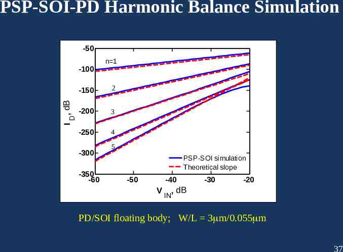
PSP-SOI-PD Harmonic Balance Simulation -50 -150 2 -200 3 -250 4 D I , dB -100 n 1 -300 -350 -60 5 PSP-SOI simulation Theoretical slope -50 -40 V IN -30 -20 , dB PD/SOI floating body; W/L 3 m/0.055 m 37
Outline PSP project overview Introduction to bulk PSP Recent development in bulk PSP PSP-SOI PSP-MGFET Conclusions 38
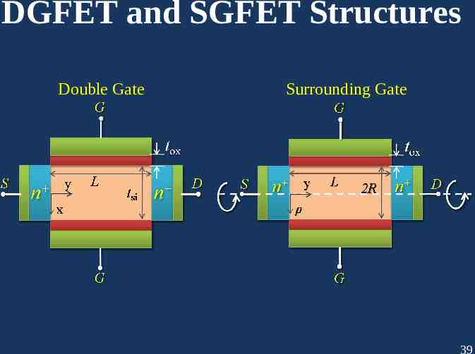
DGFET and SGFET Structures Double Gate Surrounding Gate 39
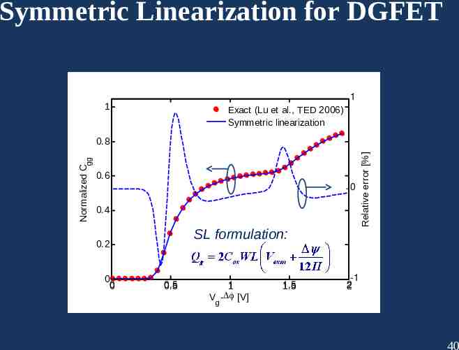
Symmetric Linearization for DGFET 1 1 Exact (Lu et al., TED 2006) Symmetric linearization 0.6 0 0.4 SL formulation: 0.2 0 0 0.5 1 V - [V] 1.5 Relative error [%] Normalized C gg 0.8 -1 2 g 40
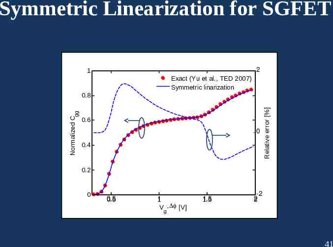
Symmetric Linearization for SGFET 1 2 Exact (Yu et al., TED 2007) Symmetric linarization 0.6 0 0.4 Relative error [%] Normalized C gg 0.8 0.2 0 0.5 1 V - [V] 1.5 -2 2 g 41
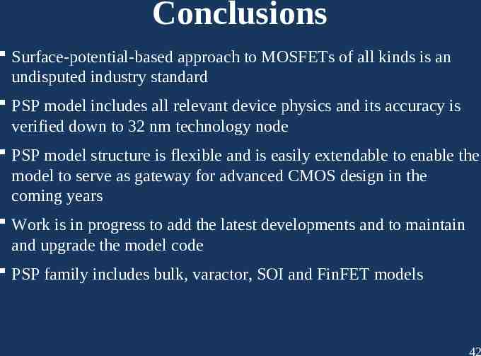
Conclusions Surface-potential-based approach to MOSFETs of all kinds is an undisputed industry standard PSP model includes all relevant device physics and its accuracy is verified down to 32 nm technology node PSP model structure is flexible and is easily extendable to enable the model to serve as gateway for advanced CMOS design in the coming years Work is in progress to add the latest developments and to maintain and upgrade the model code PSP family includes bulk, varactor, SOI and FinFET models 42
Acknowledgements PSP developers are grateful to C. McAndrew, P. Bendix, J. Watson, and G. Workman for numerous stimulating discussion of the subject of compact modeling The development of PSP is continuously funded in part by SRC since 1998 Testing and implementation of PSP is funded in part by CMC Past funding from LSI Logic, Mentor Graphics, Freescale, IBM and TI is gratefully acknowledged 43
