PRESENTATION OF ELECTRONICS-I BY : VISITING FACULTY
41 Slides686.02 KB
PRESENTATION OF ELECTRONICS-I BY : VISITING FACULTY
CHAPTER-I SEMICONDUCTOR DIODES
PN JUNCTION DIODE
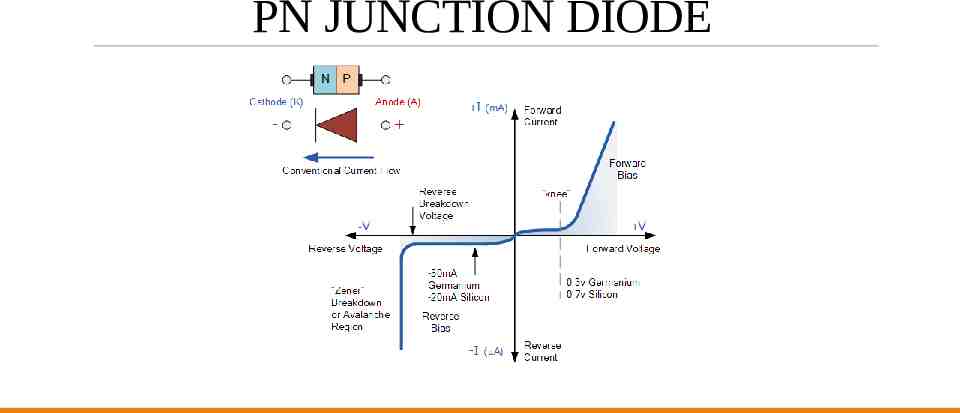
PN JUNCTION DIODE A p-n junction diode is two-terminal semiconductor device, which allows the electric current in only one direction while blocks the electric current in opposite or reverse direction. If the diode is forward biased, it allows the electric current flow. On the other hand, if the diode is reverse biased, it blocks the electric current flow. It is formed by combination of p type semiconductor and n type semiconductor. The p-n junction diode is made from the semiconductor materials such as silicon, germanium.
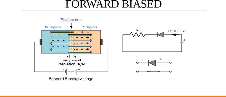
FORWARD BIASED In forward biased p-n junction diode (p-type connected to positive terminal and n-type connected to negative terminal), anode terminal is a positive terminal whereas cathode terminal is negative terminal. The free electrons are attracted towards the anode terminal or positive terminal whereas the holes are attracted towards the cathode terminal or negative terminal. With the increase in forward bias, the depletion region becomes very much thinner so that a large number of majority charge carriers can cross the PN junction and conducts an electric current. The current flowing up to built in potential is called as KNEE current.
FORWARD BIASED
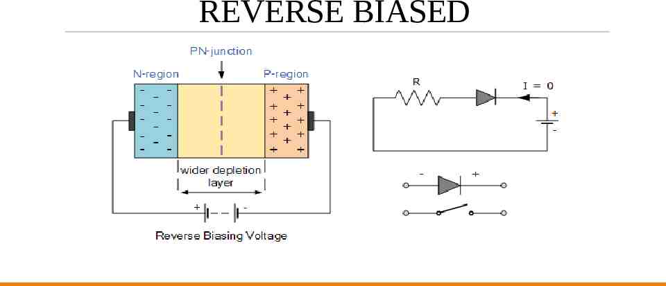
REVERSE BIASED If the diode is reverse biased (p-type connected to negative terminal and n-type connected to positive terminal), the anode terminal becomes a negative terminal whereas the cathode terminal becomes a positive terminal. The free electrons in the n-type semiconductor gets attracted towards the positive terminal. The holes from the positive terminal cannot move towards the negative terminal because the wide depletion region at the p-n junction opposes the flow of holes. The wide depletion region of reverse biased p-n junction diode completely blocks the majority charge carrier current. However, it allows the minority charge carrier current. As the reverse bias potential to the PN junction diode increases ,maximum circuit current flows in the PN junction diode. This is known as reverse breakdown voltage.
REVERSE BIASED
IDEAL DIODE An ideal diode is a diode that acts like a perfect conductor when voltage is applied forward biased and like a perfect insulator when voltage is applied reverse biased. It has infinite resistance in reverse biased condition.
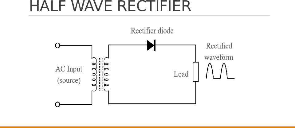
HALF WAVE RECTIFIER
WORKING The half wave rectifier is a type of rectifier that rectifies only half cycle of the waveform The half rectifier consist a step down transformer, a diode connected to the transformer and a load resistance connected to the cathode end of the diode. In the positive half cycles, diode is forward biased and allow current flowing in clock wise direction. The dc output voltage taken across load resistor In the negative half cycles, diode is reverse biased and doesnot conduct. The dc output voltage is zero.
FULL WAVE RECTIFIER A Full Wave Rectifier is a circuit, which converts an ac voltage into a pulsating dc voltage using both half cycles of the applied ac voltage. It uses two diodes of which one conducts during one half cycle while the other conducts during the other half cycle of the applied ac voltage.
TYPES OF FULL WAVE RECTIFIER There are two types of full wave rectifier Centre tapped full wave rectifier Bridge full wave rectifier
CENTRE TAPPED FULL WAVE RECTIFIER
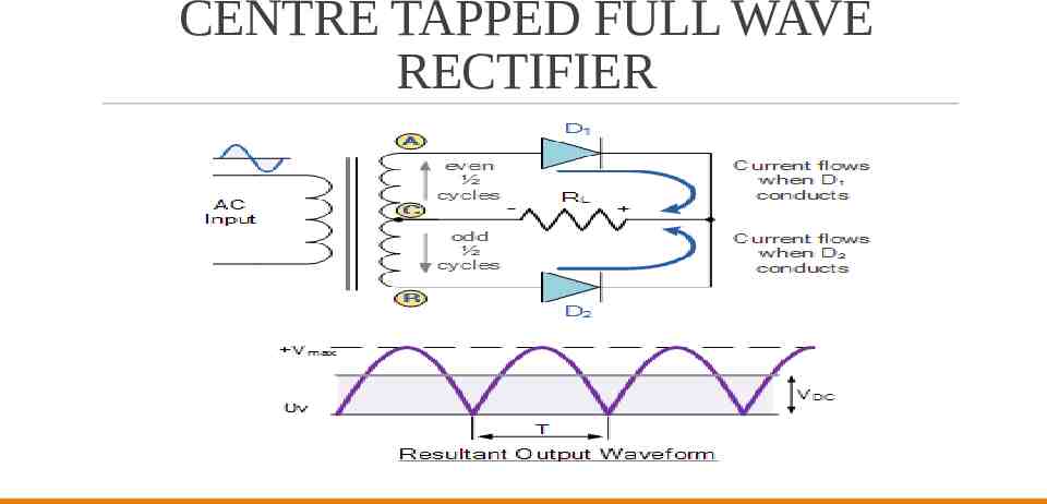
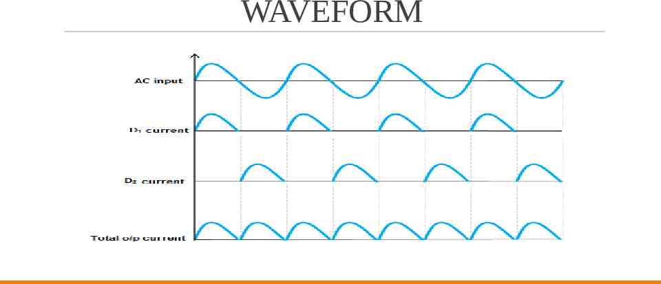
CENTRE TAPPED FULL WAVE RECTIFIER The full wave rectifier circuit consists of two power diodes connected to a single load resistance (RL). When point A of the transformer is positive with respect to point C, diode D1 conducts in the forward direction as indicated by the arrows. When point B is positive (in the negative half of the cycle) with respect to point C, diode D2 conducts in the forward direction and the current flowing through resistor R is in the same direction for both half-cycles. As the output voltage across the resistor R is the phasor sum of the two waveforms combined, this type of full wave rectifier circuit is also known as a “bi-phase” circuit.
WAVEFORM
BRIDGE FULL WAVE RECTIFIER
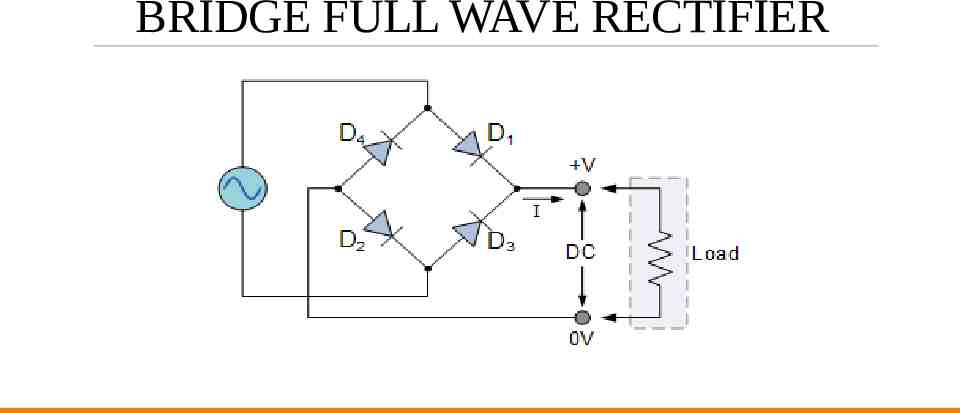
BRIDGE FULL WAVE RECTIFIER The four diodes labelled D1 to D4 are arranged in “series pairs” with only two diodes conducting current during each half cycle. During the positive half cycle of the supply, diodes D1 and D2 conduct in series while diodes D3 and D4 are reverse biased and the current flows through the load During the negative half cycle of the supply, diodes D3 and D4 conduct in series, but diodes D1 and D2 switch “OFF” as they are now reverse biased. The current flowing through the load is the same direction as before.
FILTER AND TYPES OF FILTER The filter is a device that allows passing the dc component of the load and blocks the ac component of the rectifier output. Thus the output of the filter circuit will be a steady dc voltage. TYPES OF FILTER Shunt capacitor filter Series inductor filter LC filter Pie filter
TYPES OF DIODES Different types of diodes are: Zener diode Varactor diode Schottky diode Light emitting diode Photo diode
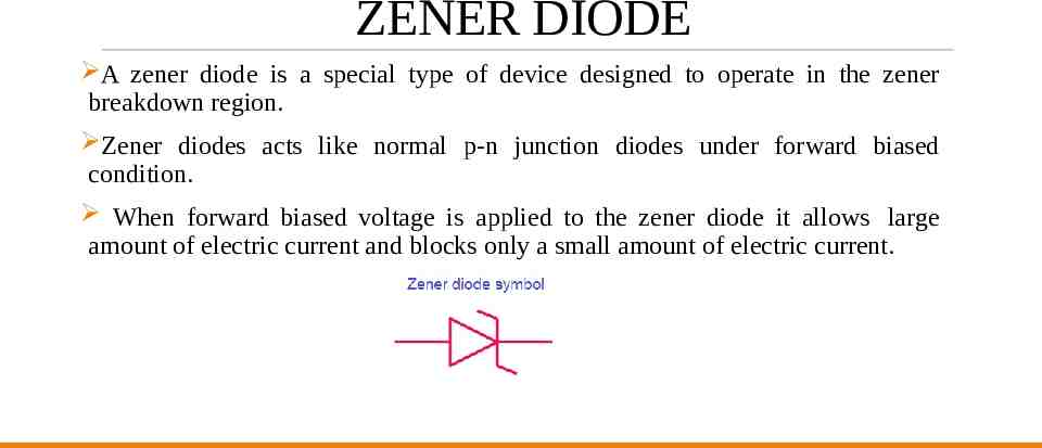
ZENER DIODE A zener diode is a special type of device designed to operate in the zener breakdown region. Zener diodes acts like normal p-n junction diodes under forward biased condition. When forward biased voltage is applied to the zener diode it allows large amount of electric current and blocks only a small amount of electric current.
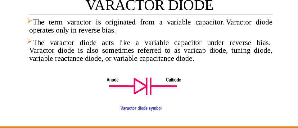
VARACTOR DIODE The term varactor is originated from a variable capacitor. Varactor diode operates only in reverse bias. The varactor diode acts like a variable capacitor under reverse bias. Varactor diode is also sometimes referred to as varicap diode, tuning diode, variable reactance diode, or variable capacitance diode.
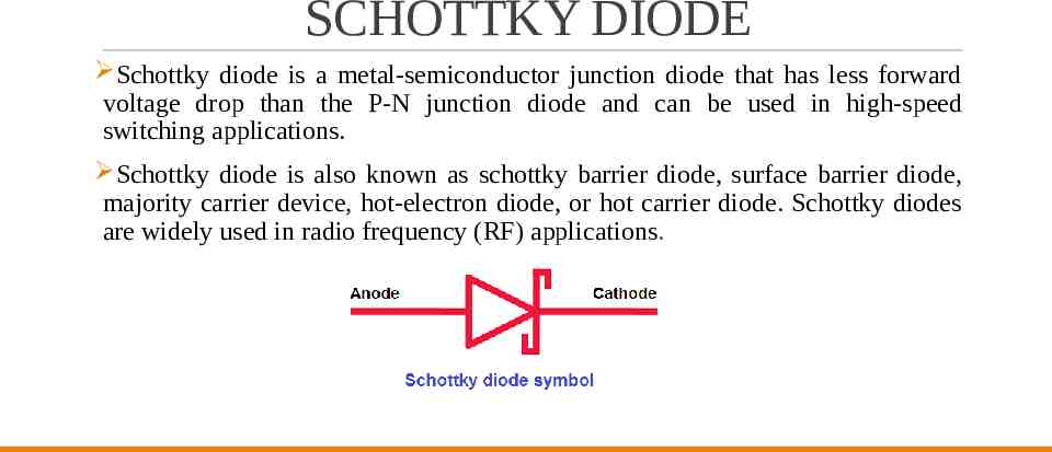
SCHOTTKY DIODE Schottky diode is a metal-semiconductor junction diode that has less forward voltage drop than the P-N junction diode and can be used in high-speed switching applications. Schottky diode is also known as schottky barrier diode, surface barrier diode, majority carrier device, hot-electron diode, or hot carrier diode. Schottky diodes are widely used in radio frequency (RF) applications.
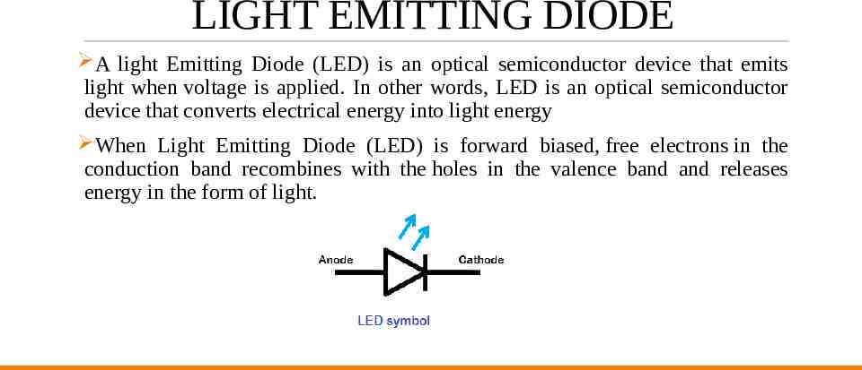
LIGHT EMITTING DIODE A light Emitting Diode (LED) is an optical semiconductor device that emits light when voltage is applied. In other words, LED is an optical semiconductor device that converts electrical energy into light energy When Light Emitting Diode (LED) is forward biased, free electrons in the conduction band recombines with the holes in the valence band and releases energy in the form of light.
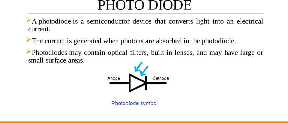
PHOTO DIODE A photodiode is a semiconductor device that converts light into an electrical current. The current is generated when photons are absorbed in the photodiode. Photodiodes may contain optical filters, built-in lenses, and may have large or small surface areas.
ZENER DIODE AS VOLTAGE REGULATOR
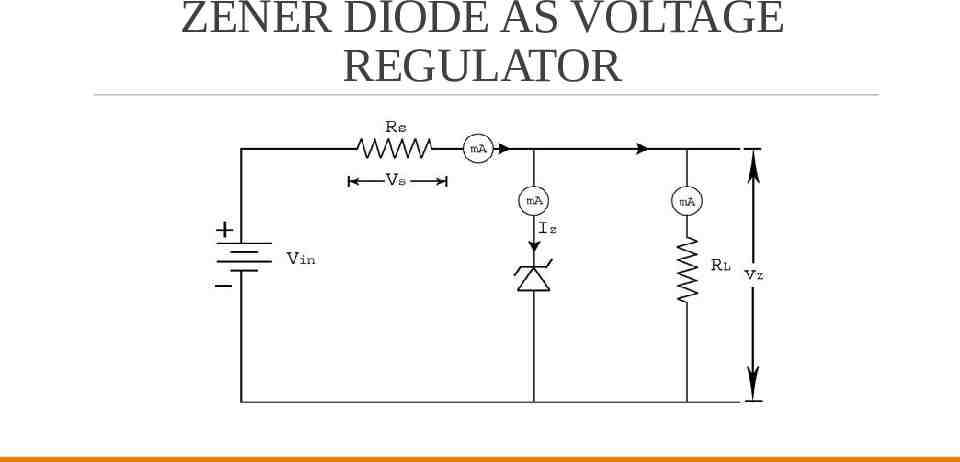
ZENER DIODE AS VOLTAGE REGULATOR The function of a regulator is to provide a constant output voltage to a load connected in parallel with it in spite of the ripples in the supply voltage or the variation in the load current and the zener diode will continue to regulate the voltage until the diodes current falls below the minimum I Z(min) value in the reverse breakdown region. It permits current to flow in the forward direction as normal, but will also allow it to flow in the reverse direction when the voltage is above a certain value - the breakdown voltage known as the Zener voltage. The resistor is selected so that when the input voltage is at V IN(min) and the load current is at IL(max) that the current through the Zener diode is at least Iz(min). A zener diode of break down voltage Vz is reverse connected to an input voltage source V i across a load resistance RL and a series resistor RS. The voltage across the zener will remain steady at its break down voltage VZ for all the values of zener current IZ as long as the current remains in the break down region. Hence a regulated DC output voltage V0 VZ is obtained across RL, whenever the input voltage remains within a minimum and maximum voltage.
CHAPTER-2 BIPOLAR TRANSISTORS
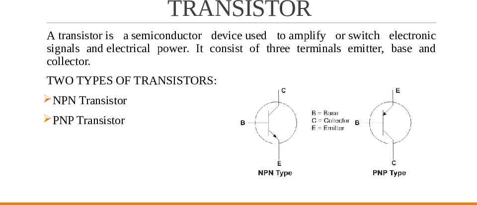
TRANSISTOR A transistor is a semiconductor device used to amplify or switch electronic signals and electrical power. It consist of three terminals emitter, base and collector. TWO TYPES OF TRANSISTORS: NPN Transistor PNP Transistor
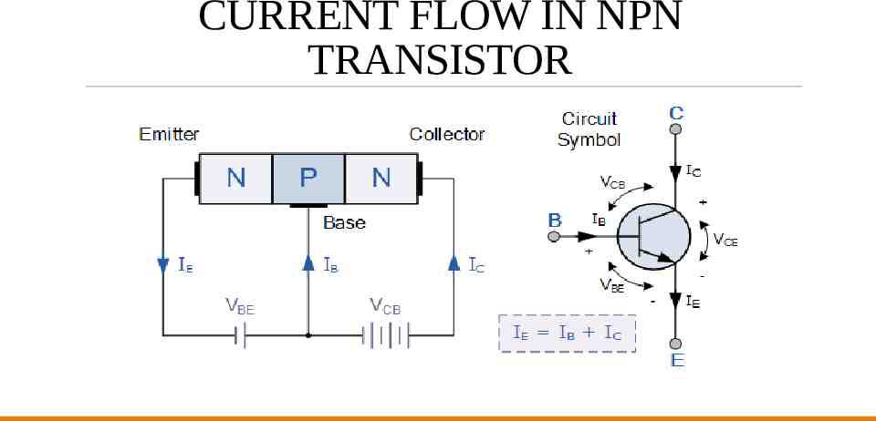
CURRENT FLOW IN NPN TRANSISTOR
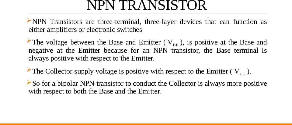
NPN TRANSISTOR NPN Transistors are three-terminal, three-layer devices that can function as either amplifiers or electronic switches The voltage between the Base and Emitter ( VBE ), is positive at the Base and negative at the Emitter because for an NPN transistor, the Base terminal is always positive with respect to the Emitter. The Collector supply voltage is positive with respect to the Emitter ( VCE ). So for a bipolar NPN transistor to conduct the Collector is always more positive with respect to both the Base and the Emitter.
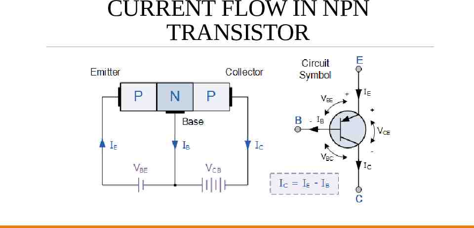
CURRENT FLOW IN NPN TRANSISTOR
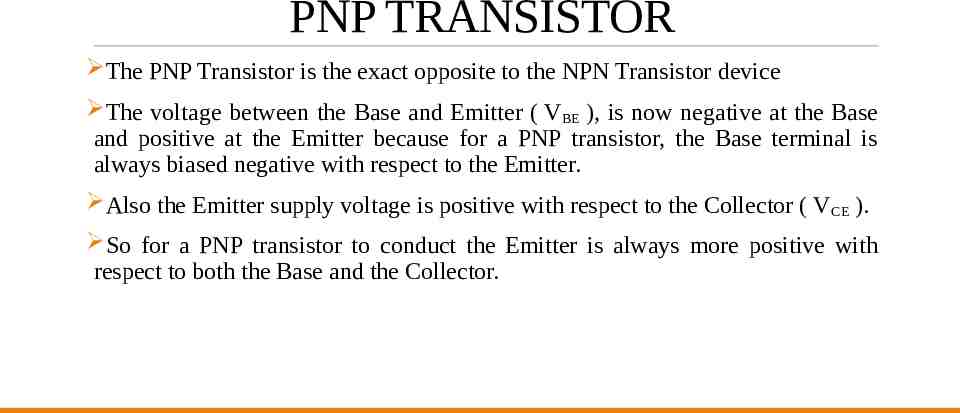
PNP TRANSISTOR The PNP Transistor is the exact opposite to the NPN Transistor device The voltage between the Base and Emitter ( VBE ), is now negative at the Base and positive at the Emitter because for a PNP transistor, the Base terminal is always biased negative with respect to the Emitter. Also the Emitter supply voltage is positive with respect to the Collector ( VCE ). So for a PNP transistor to conduct the Emitter is always more positive with respect to both the Base and the Collector.
TYPES OF TRANSISTOR CONFIGURATIONS There are three types of transistor configuration: Common base configuration(CB) Common emitter configuration(CE) Common collector configuration(CC)
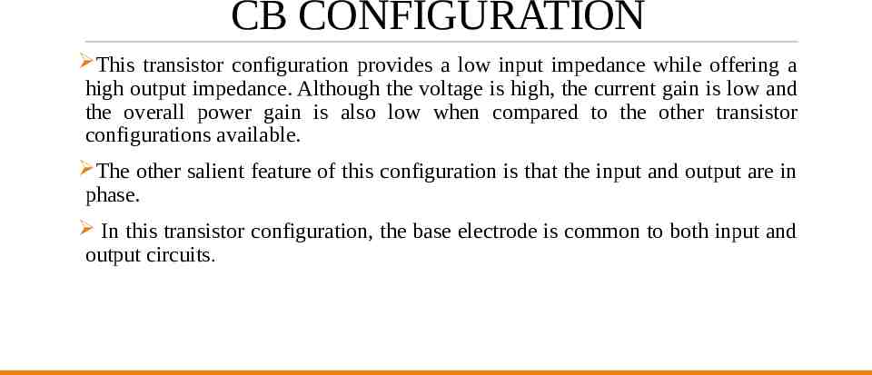
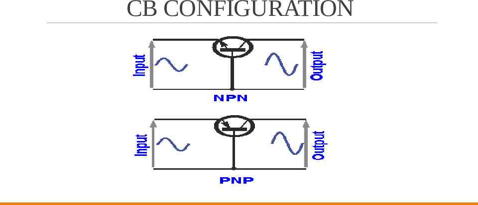
CB CONFIGURATION This transistor configuration provides a low input impedance while offering a high output impedance. Although the voltage is high, the current gain is low and the overall power gain is also low when compared to the other transistor configurations available. The other salient feature of this configuration is that the input and output are in phase. In this transistor configuration, the base electrode is common to both input and output circuits.
CB CONFIGURATION
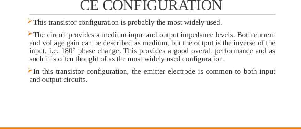
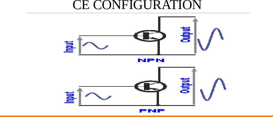
CE CONFIGURATION This transistor configuration is probably the most widely used. The circuit provides a medium input and output impedance levels. Both current and voltage gain can be described as medium, but the output is the inverse of the input, i.e. 180 phase change. This provides a good overall performance and as such it is often thought of as the most widely used configuration. In this transistor configuration, the emitter electrode is common to both input and output circuits.
CE CONFIGURATION
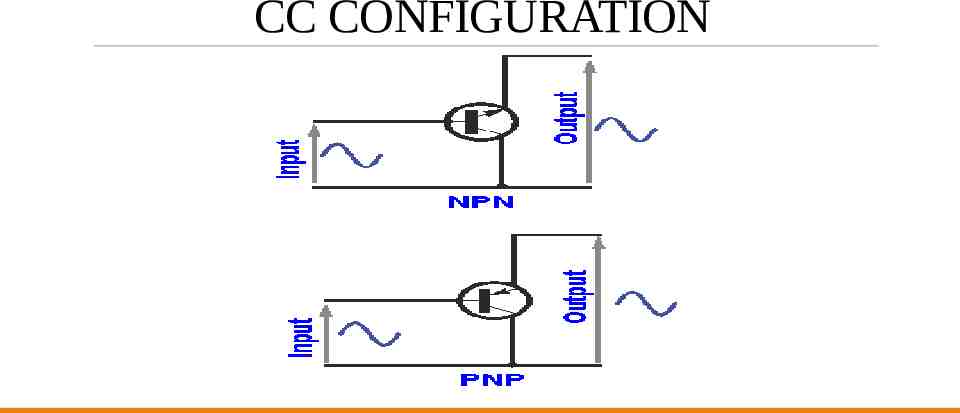
CC CONFIGURATION This transistor configuration is also known as the emitter follower because the emitter voltage follows that of the base. Offering a high input impedance and a low output impedance it is widely used as a buffer. The voltage gain is unity, although current gain is high. The input and output signals are in phase. In this transistor configuration, the collector electrode is common to both input and output circuits.
CC CONFIGURATION
THANK YOU SUBMITTED BY: POOJA MALIK

