Low Power VLSI Design and Tools Subhomoy Chattopadhyay and Rakesh
87 Slides763.50 KB
Low Power VLSI Design and Tools Subhomoy Chattopadhyay and Rakesh Patel WCCG/ICG Intel Corporation, Chandler,AZ,USA. ASPDAC Seminar 1
Outline of the Tutorial 9.00: 9:15 Introduction and motivation, sources of dissipation Active power reduction methods 9:15-9.30 09:30-10.00 Power reduction in clocking circuits,buses etc 10.0 -10:15 Low power domino, SRAM design and leakage power reduction 10:15 -10:25 Conclusion and final thoughts 10:25-10:35 Q & A, Break Power Analysis and Optimization tools and 10:35-1:00 methodology ASPDAC Seminar 2
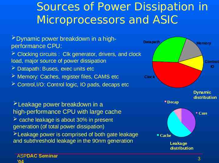
Sources of Power Dissipation in Microprocessors and ASIC Dynamic power breakdown in a highperformance CPU: Clocking circuits : Clk generator, drivers, and clock load, major source of power dissipation Datapath: Buses, exec units etc Memory: Caches, register files, CAMS etc Control,I/O: Control logic, IO pads, decaps etc Datapath Memory Control, IO Clock Dynamic distribution Leakage power breakdown in a high-performance CPU with large cache cache leakage is about 30% in present generation (of total power dissipation) Leakage power is comprised of both gate leakage and subthreshold leakage in the 90nm generation ASPDAC Seminar Decap Core Cache Leakage distribution 3
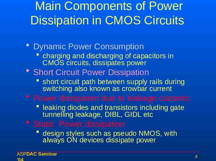
Main Components of Power Dissipation in CMOS Circuits Dynamic Power Consumption charging and discharging of capacitors in CMOS circuits, dissipates power Short Circuit Power Dissipation short circuit path between supply rails during switching also known as crowbar current Power dissipation due to leakage currents leaking diodes and transistors including gate tunnelling leakage, DIBL, GIDL etc Static Power dissipation design styles such as pseudo NMOS, with always ON devices dissipate power ASPDAC Seminar 4
Problems Associated with higher Power Dissipation CMOS is no longer low-power (100 W for P’s of today) Bigger concern than performance in some applications, results in lower voltage to meet power envelope at the expense of speed Difficult to supply large amount of current into/out of a chip 100W at 1.25V 80A Cost of packaging goes up – because of higher current Want to use plastic packages for low-cost Cooling is difficult for most applications except servers Portable systems Need to carry energy (in battery) More power means longer-lasting, heavier batteries needed or frequent charging needed especially in PDAs and cell phones ASPDAC Seminar 5
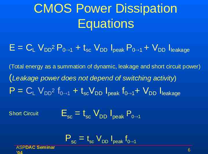
CMOS Power Dissipation Equations E CL VDD2 P0 1 tsc VDD Ipeak P0 1 VDD Ileakage (Total energy as a summation of dynamic, leakage and short circuit power) (Leakage power does not depend of switching activity) P CL VDD2 f0 1 tscVDD Ipeak f0 1 VDD Ileakage Short Circuit Esc tsc VDD Ipeak P0 1 Psc tsc VDD Ipeak f0 1 ASPDAC Seminar 6
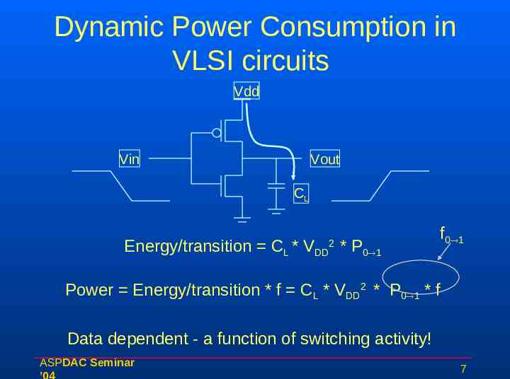
Dynamic Power Consumption in VLSI circuits Vdd Vin Vout CL Energy/transition CL * V 2 DD * P0 1 f0 1 Power Energy/transition * f CL * VDD2 * P0 1 * f Data dependent - a function of switching activity! ASPDAC Seminar 7
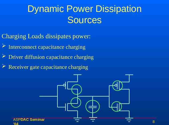
Dynamic Power Dissipation Sources Charging Loads dissipates power: Interconnect capacitance charging Driver diffusion capacitance charging Receiver gate capacitance charging ASPDAC Seminar 8
Basic tips for Lowering Dynamic Power Reducing VDD has a quadratic effect! However reducing VDD has a negative effect on performance especially as VDD approaches 2 times Vt. Lowering CL Improves performance as well as power Keep transistors minimum size (keeps intrinsic capacitance (gate and diffusion) small) Transistors should be sized only when CL is dominated by extrinsic capacitance (fanout and wires) Reducing the switching activity, f0 1 P0 1 * f A function of signal statistics and clock rate Impacted by logic and architecture design decisions ASPDAC Seminar 9
Circuit Techniques to Reduce power Circuit family selection is very important ! static vs. domino circuits ? Use static wherever timing permits unless : – Very efficient clock gating has been implemented Circuit active 20% of the time, domino okay if clock is off most of the time – The AF of all/most signals is 0.3 Domino circuits have an advantage due to lower capacitance in domino because of absence of PFETs. For lower AF domino ok also Domino circuits require clock and extra routing but : – Have smaller size, lower input capacitance and are faster ASPDAC Seminar 10
Circuit Sizing Techniques Circuit sizing is very important for both active and leakage power reduction Downsize latches and flip-flops in design : clocks and sequentials dissipate 70% of total power (IBM Power4 processor design)( includes distribution) There is no need for large sized sequentials, size down Buffer clocks to sequentials if possible to reduce clock loading, timing may be an issue here Use the electrical rule checks and queries for – timing – output AF, to help downsize decisions Use circuit sizing tool like AMPS from Synopsys early in the design cycle to downsize ASPDAC Seminar 11
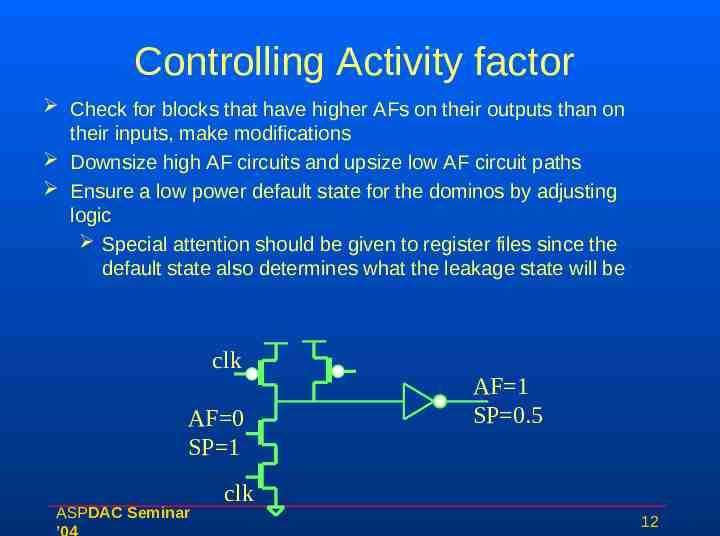
Controlling Activity factor Check for blocks that have higher AFs on their outputs than on their inputs, make modifications Downsize high AF circuits and upsize low AF circuit paths Ensure a low power default state for the dominos by adjusting logic Special attention should be given to register files since the default state also determines what the leakage state will be clk AF 0 SP 1 ASPDAC Seminar AF 1 SP 0.5 clk 12
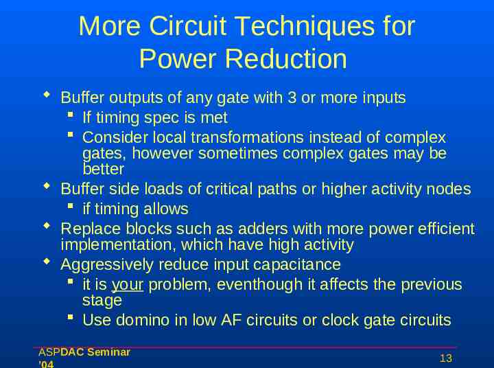
More Circuit Techniques for Power Reduction Buffer outputs of any gate with 3 or more inputs If timing spec is met Consider local transformations instead of complex gates, however sometimes complex gates may be better Buffer side loads of critical paths or higher activity nodes if timing allows Replace blocks such as adders with more power efficient implementation, which have high activity Aggressively reduce input capacitance it is your problem, eventhough it affects the previous stage Use domino in low AF circuits or clock gate circuits ASPDAC Seminar 13
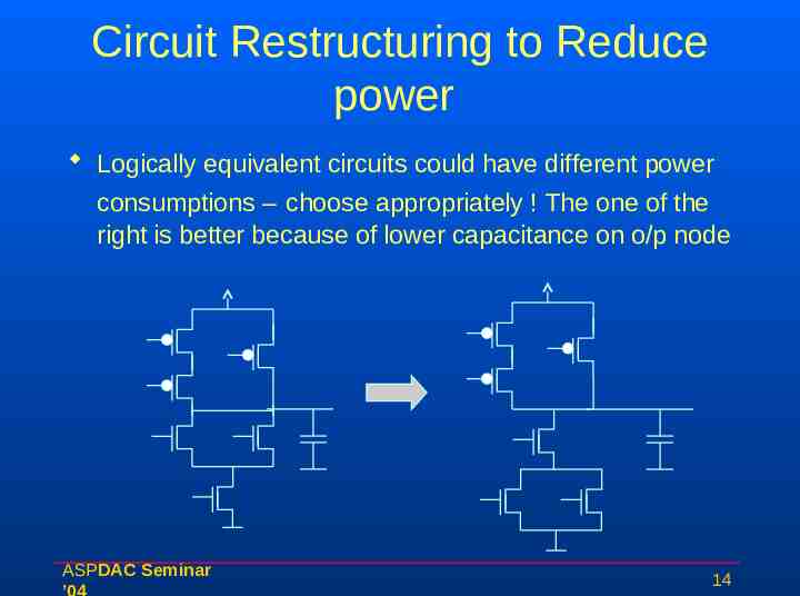
Circuit Restructuring to Reduce power Logically equivalent circuits could have different power consumptions – choose appropriately ! The one of the right is better because of lower capacitance on o/p node ASPDAC Seminar 14
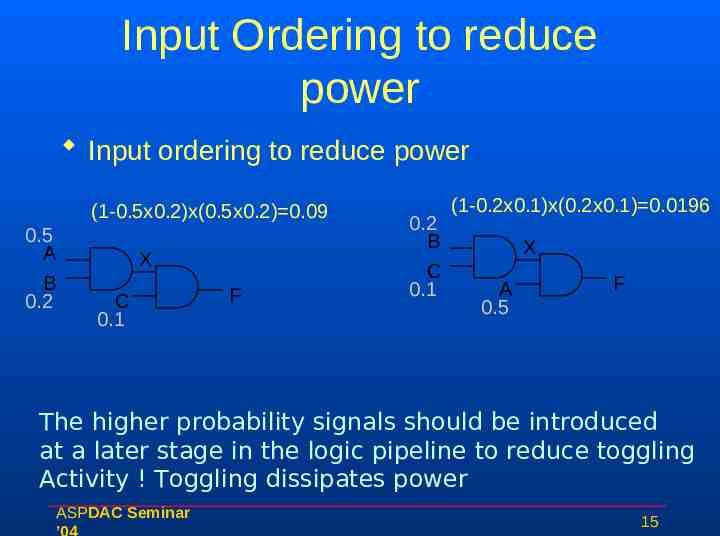
Input Ordering to reduce power Input ordering to reduce power (1-0.5x0.2)x(0.5x0.2) 0.09 0.5 A B 0.2 X C 0.1 F 0.2 B C 0.1 (1-0.2x0.1)x(0.2x0.1) 0.0196 X A 0.5 F The higher probability signals should be introduced at a later stage in the logic pipeline to reduce toggling Activity ! Toggling dissipates power ASPDAC Seminar 15
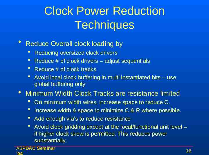
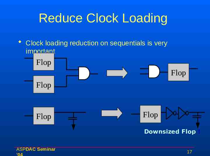
Clock Power Reduction Techniques Reduce Overall clock loading by Reducing oversized clock drivers Reduce # of clock drivers – adjust sequentials Reduce # of clock tracks Avoid local clock buffering in multi instantiated bits – use global buffering only Minimum Width Clock Tracks are resistance limited On minimum width wires, increase space to reduce C. Increase width & space to minimize C & R where possible. Add enough via’s to reduce resistance Avoid clock gridding except at the local/functional unit level – if higher clock skew is permitted. This reduces power substantially. ASPDAC Seminar 16
Reduce Clock Loading Clock loading reduction on sequentials is very important Flop Flop Flop Flop Flop Downsized Flop ! ASPDAC Seminar 17
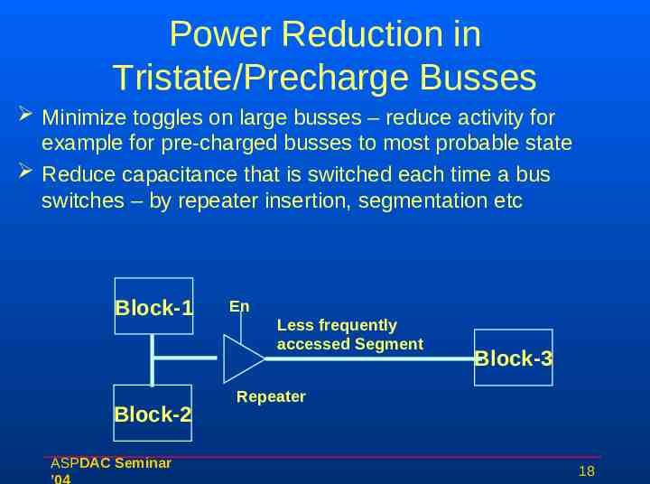
Power Reduction in Tristate/Precharge Busses Minimize toggles on large busses – reduce activity for example for pre-charged busses to most probable state Reduce capacitance that is switched each time a bus switches – by repeater insertion, segmentation etc Block-1 Block-2 ASPDAC Seminar En Less frequently accessed Segment Block-3 Repeater 18
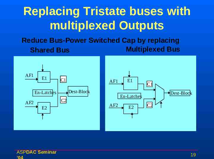
Replacing Tristate buses with multiplexed Outputs Reduce Bus-Power Switched Cap by replacing Multiplexed Bus Shared Bus AF1 E1 C1 C1 Dest-Block En-Latches C2 AF2 E2 ASPDAC Seminar AF1 E1 C1 Dest-Block En-Latches AF2 E2 C2 19
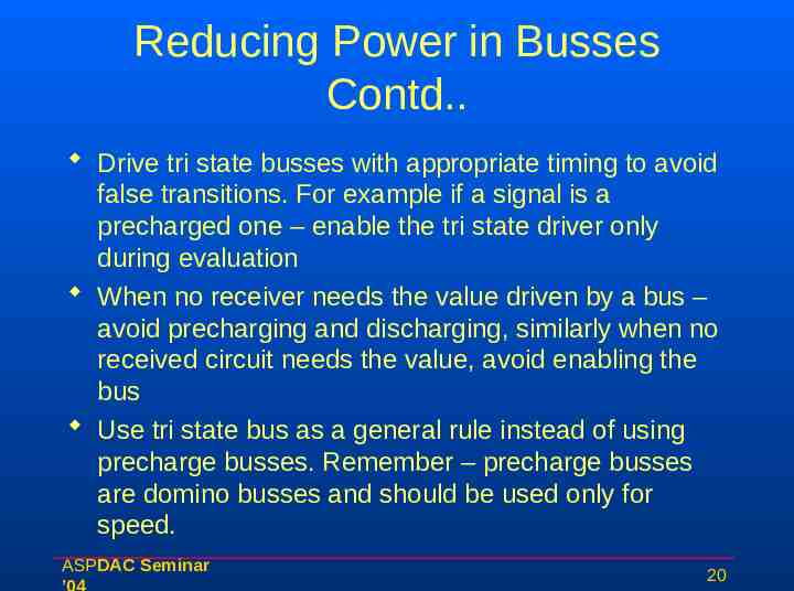
Reducing Power in Busses Contd. Drive tri state busses with appropriate timing to avoid false transitions. For example if a signal is a precharged one – enable the tri state driver only during evaluation When no receiver needs the value driven by a bus – avoid precharging and discharging, similarly when no received circuit needs the value, avoid enabling the bus Use tri state bus as a general rule instead of using precharge busses. Remember – precharge busses are domino busses and should be used only for speed. ASPDAC Seminar 20
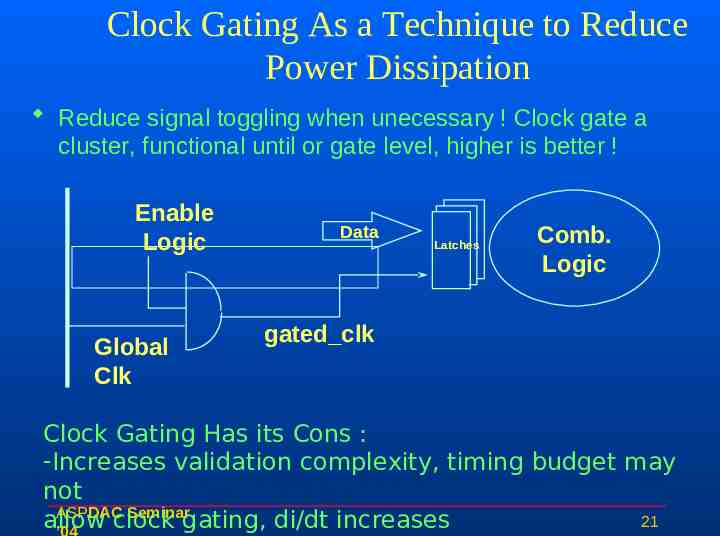
Clock Gating As a Technique to Reduce Power Dissipation Reduce signal toggling when unecessary ! Clock gate a cluster, functional until or gate level, higher is better ! Enable Logic Global Clk Data Latches Comb. Logic gated clk Clock Gating Has its Cons : -Increases validation complexity, timing budget may not ASPDAC Seminar 21 allow clock gating, di/dt increases
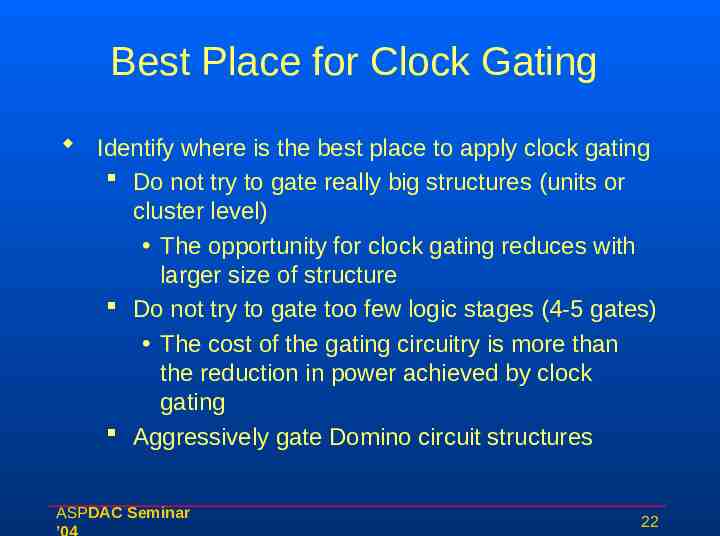
Best Place for Clock Gating Identify where is the best place to apply clock gating Do not try to gate really big structures (units or cluster level) The opportunity for clock gating reduces with larger size of structure Do not try to gate too few logic stages (4-5 gates) The cost of the gating circuitry is more than the reduction in power achieved by clock gating Aggressively gate Domino circuit structures ASPDAC Seminar 22
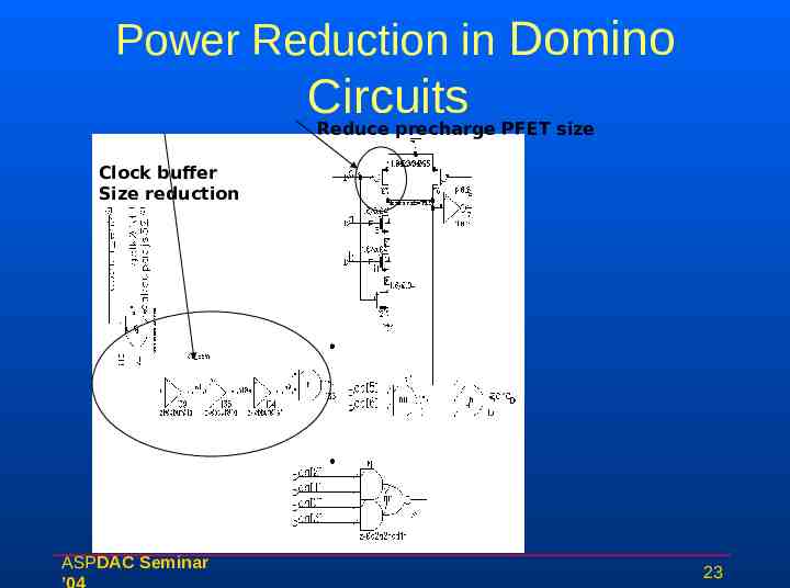
Power Reduction in Domino Circuits Reduce precharge PFET size Clock buffer Size reduction ASPDAC Seminar 23
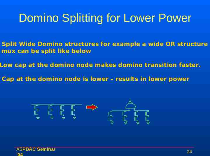
Domino Splitting for Lower Power Split Wide Domino structures for example a wide OR structure l mux can be split like below Low cap at the domino node makes domino transition faster. Cap at the domino node is lower – results in lower power ASPDAC Seminar 24
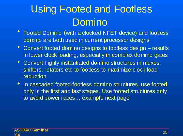
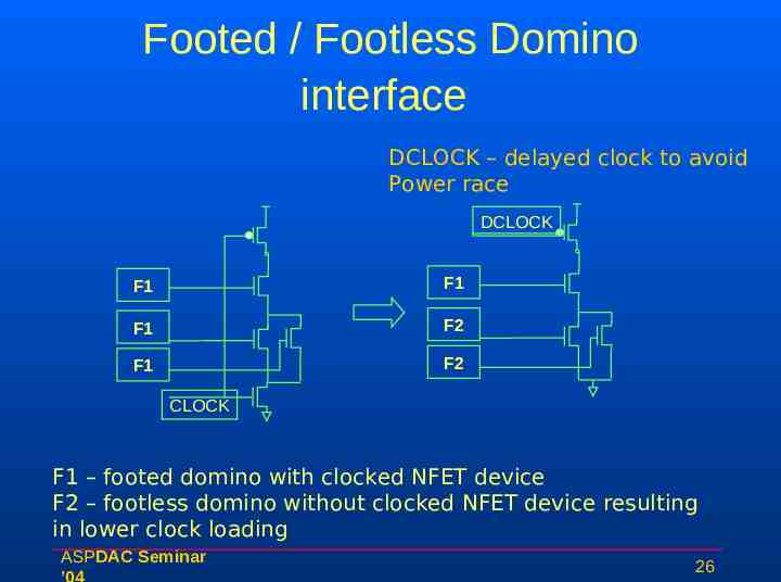
Using Footed and Footless Domino Footed Domino (with a clocked NFET device) and footless domino are both used in current processor designs Convert footed domino designs to footless design – results in lower clock loading, especially in complex domino gates Convert highly instantiated domino structures in muxes, shifters, rotators etc to footless to maximize clock load reduction In cascaded footed-footless domino structures, use footed only in the first and last stages. Use footed structures only to avoid power races example next page ASPDAC Seminar 25
Footed / Footless Domino interface DCLOCK – delayed clock to avoid Power race DCLOCK F1 F1 F1 F2 F1 F2 CLOCK F1 – footed domino with clocked NFET device F2 – footless domino without clocked NFET device resulting in lower clock loading ASPDAC Seminar 26
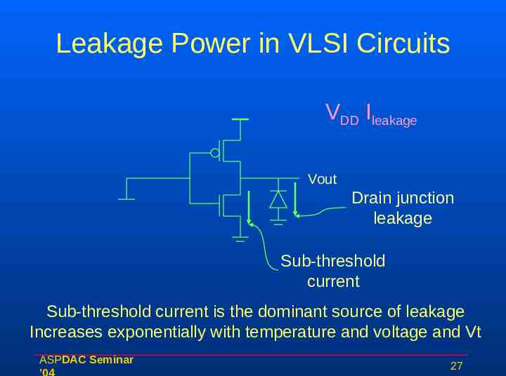
Leakage Power in VLSI Circuits VDD Ileakage Vout Drain junction leakage Sub-threshold current Sub-threshold current is the dominant source of leakage Increases exponentially with temperature and voltage and Vt ASPDAC Seminar 27
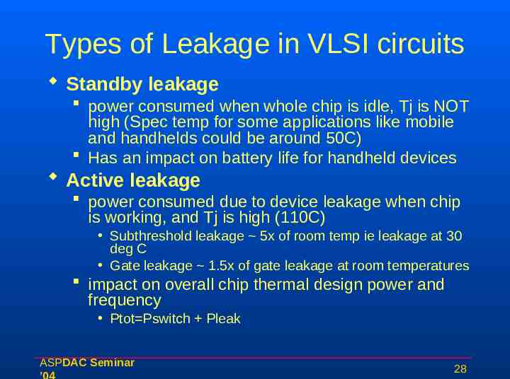
Types of Leakage in VLSI circuits Standby leakage power consumed when whole chip is idle, Tj is NOT high (Spec temp for some applications like mobile and handhelds could be around 50C) Has an impact on battery life for handheld devices Active leakage power consumed due to device leakage when chip is working, and Tj is high (110C) Subthreshold leakage 5x of room temp ie leakage at 30 deg C Gate leakage 1.5x of gate leakage at room temperatures impact on overall chip thermal design power and frequency Ptot Pswitch Pleak ASPDAC Seminar 28
Leakage Reduction Methods Methods to reduce leakage in CMOS VLSI circuits Longer Leff (one or half grid more than nominal) Dual Vcc in the cores – use regulators on chip Forcing stacked structures reduces leakage, mostly in low AF circuits like memories, RF Dual Vt – has to be supported by the process Sleep control transistors – more details in later foils Back bias – body back bias in NFET and PFET transistors to reduce leakage by upto 3x with appropriate body bias. NFET leakage is dominant Sizing down to reduce both active and leakage power ASPDAC Seminar 29
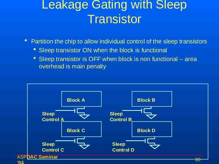
Leakage Gating with Sleep Transistor Partition the chip to allow individual control of the sleep transistors Sleep transistor ON when the block is functional Sleep transistor is OFF when block is non functional – area overhead is main penalty Block A Sleep Control A Block B Sleep Control B Block C Sleep Control C ASPDAC Seminar Block D Sleep Control D 30
Some More Leakage Reduction Techniques Body Biasing Increase Vt by reverse-biased body effect(RBB) Large transition time and wakeup latency due to well cap and resistance Power Gating Inserting longer L transistor in non timing critical paths to reduce leakage – based on static timing analysis runs for functional units Removal of low Vt transistors – at the expense of speed to reduce leakage Sleep Vector based reduction Input vector which minimizes leakage Increased delay due to mux and active energy due to spurious toggles after applying sleep vector ASPDAC Seminar 31
Low Power Memory design Challenge On chip cache size increasing substantially in modern microprocessors for greater performance – 6MB L2 cache in Itanium 2 processor Increase in cache size results in higher leakage power (predominantly) in 90nm and smaller geometries – activity factor for large caches very low and hence active power is not the major source of power dissipation Gate leakage will dominate leakage in caches in the 65nm and smaller geometries – standby subthreshold leakage already low because of non minimum L used. Leakage power reduction in caches will be a challenge for designers in 90nm and smaller geometries ! ASPDAC Seminar 32
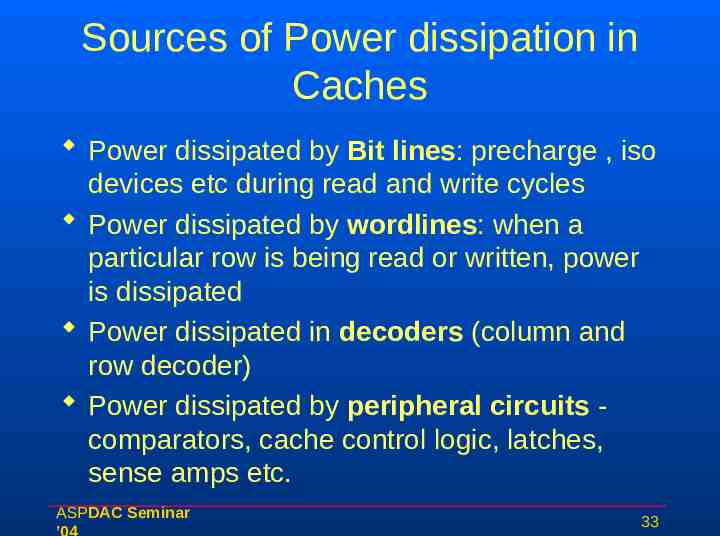
Sources of Power dissipation in Caches Power dissipated by Bit lines: precharge , iso devices etc during read and write cycles Power dissipated by wordlines: when a particular row is being read or written, power is dissipated Power dissipated in decoders (column and row decoder) Power dissipated by peripheral circuits comparators, cache control logic, latches, sense amps etc. ASPDAC Seminar 33
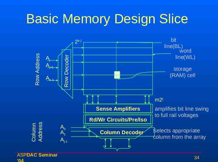
Basic Memory Design Slice bit line(BL) word line(WL) Aj Aj 1 Ak-1 Row Decoder Row Address 2k-j storage (RAM) cell m2j Column Address Sense Amplifiers ASPDAC Seminar Rd/Wr Circuits/Pre/Iso A0 A1 Aj-1 Column Decoder amplifies bit line swing to full rail voltages Selects appropriate column from the array 34
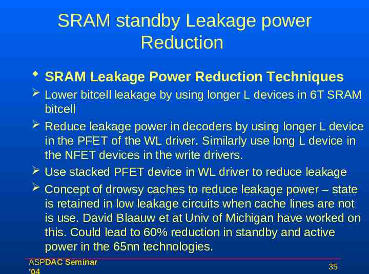
SRAM standby Leakage power Reduction SRAM Leakage Power Reduction Techniques Lower bitcell leakage by using longer L devices in 6T SRAM bitcell Reduce leakage power in decoders by using longer L device in the PFET of the WL driver. Similarly use long L device in the NFET devices in the write drivers. Use stacked PFET device in WL driver to reduce leakage Concept of drowsy caches to reduce leakage power – state is retained in low leakage circuits when cache lines are not is use. David Blaauw et at Univ of Michigan have worked on this. Could lead to 60% reduction in standby and active power in the 65nn technologies. ASPDAC Seminar 35
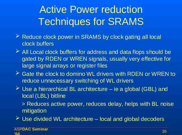
Active Power reduction Techniques for SRAMS Reduce clock power in SRAMS by clock gating all local clock buffers All Local clock buffers for address and data flops should be gated by RDEN or WREN signals, usually very effective for large signal arrays or register files Gate the clock to domino WL drivers with RDEN or WREN to reduce unnecessary switching of WL drivers Use a hierarchical BL architecture – ie a global (GBL) and local (LBL) bitline Reduces active power, reduces delay, helps with BL noise mitigation Use divided WL architecture – local and global decoders ASPDAC Seminar 36
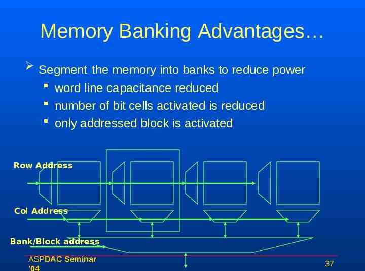
Memory Banking Advantages Segment the memory into banks to reduce power word line capacitance reduced number of bit cells activated is reduced only addressed block is activated Row Address Col Address Bank/Block address ASPDAC Seminar 37
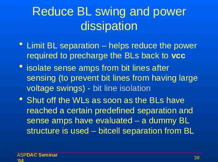
Reduce BL swing and power dissipation Limit BL separation – helps reduce the power required to precharge the BLs back to vcc isolate sense amps from bit lines after sensing (to prevent bit lines from having large voltage swings) - bit line isolation Shut off the WLs as soon as the BLs have reached a certain predefined separation and sense amps have evaluated – a dummy BL structure is used – bitcell separation from BL ASPDAC Seminar 38
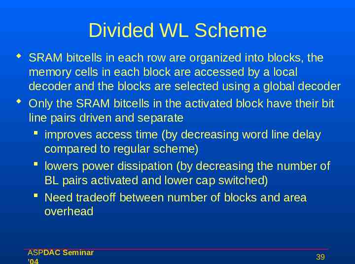
Divided WL Scheme SRAM bitcells in each row are organized into blocks, the memory cells in each block are accessed by a local decoder and the blocks are selected using a global decoder Only the SRAM bitcells in the activated block have their bit line pairs driven and separate improves access time (by decreasing word line delay compared to regular scheme) lowers power dissipation (by decreasing the number of BL pairs activated and lower cap switched) Need tradeoff between number of blocks and area overhead ASPDAC Seminar 39
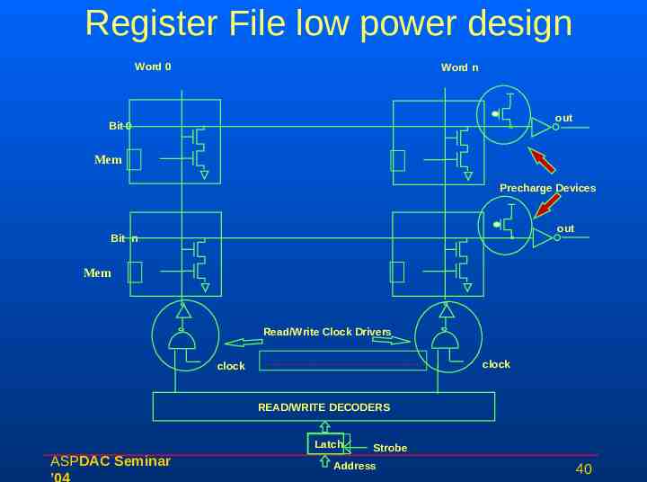
Register File low power design Word 0 Word n out Bit 0 Mem Precharge Devices out Bit n Mem Read/Write Clock Drivers clock . clock READ/WRITE DECODERS Latch ASPDAC Seminar Strobe Address 40
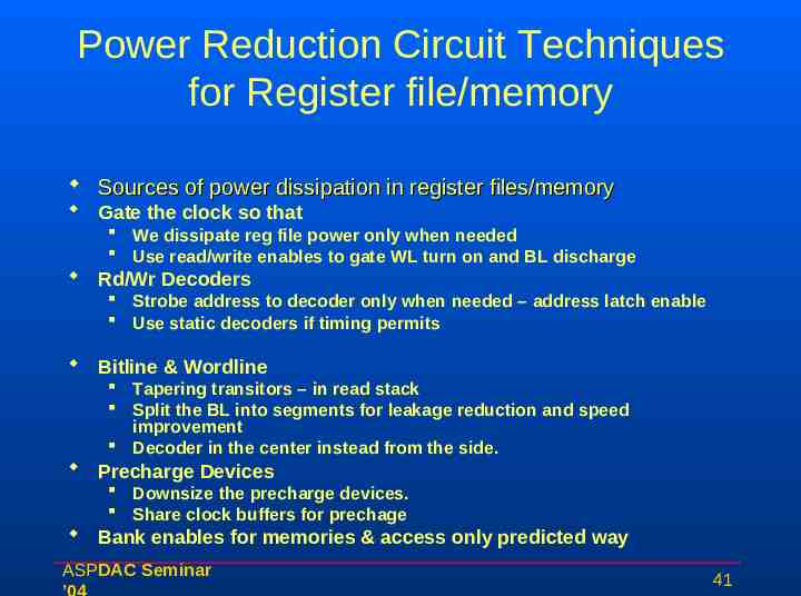
Power Reduction Circuit Techniques for Register file/memory Sources of power dissipation in register files/memory Gate the clock so that We dissipate reg file power only when needed Use read/write enables to gate WL turn on and BL discharge Rd/Wr Decoders Strobe address to decoder only when needed – address latch enable Use static decoders if timing permits Bitline & Wordline Tapering transitors – in read stack Split the BL into segments for leakage reduction and speed improvement Decoder in the center instead from the side. Precharge Devices Downsize the precharge devices. Share clock buffers for prechage Bank enables for memories & access only predicted way ASPDAC Seminar 41
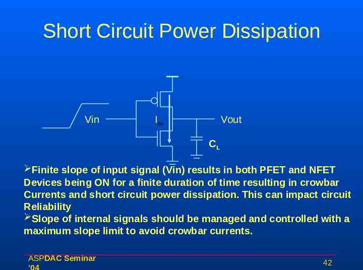
Short Circuit Power Dissipation Vin Isc Vout CL Finite slope of input signal (Vin) results in both PFET and NFET Devices being ON for a finite duration of time resulting in crowbar Currents and short circuit power dissipation. This can impact circuit Reliability Slope of internal signals should be managed and controlled with a maximum slope limit to avoid crowbar currents. ASPDAC Seminar 42
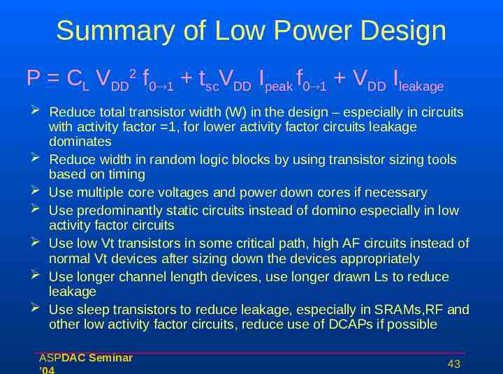
Summary of Low Power Design P CL VDD2 f0 1 tscVDD Ipeak f0 1 VDD Ileakage Reduce total transistor width (W) in the design – especially in circuits with activity factor 1, for lower activity factor circuits leakage dominates Reduce width in random logic blocks by using transistor sizing tools based on timing Use multiple core voltages and power down cores if necessary Use predominantly static circuits instead of domino especially in low activity factor circuits Use low Vt transistors in some critical path, high AF circuits instead of normal Vt devices after sizing down the devices appropriately Use longer channel length devices, use longer drawn Ls to reduce leakage Use sleep transistors to reduce leakage, especially in SRAMs,RF and other low activity factor circuits, reduce use of DCAPs if possible ASPDAC Seminar 43
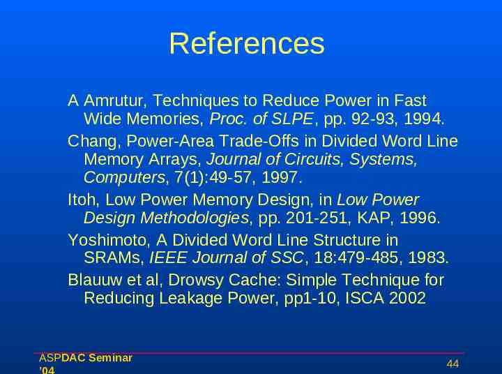
References A Amrutur, Techniques to Reduce Power in Fast Wide Memories, Proc. of SLPE, pp. 92-93, 1994. Chang, Power-Area Trade-Offs in Divided Word Line Memory Arrays, Journal of Circuits, Systems, Computers, 7(1):49-57, 1997. Itoh, Low Power Memory Design, in Low Power Design Methodologies, pp. 201-251, KAP, 1996. Yoshimoto, A Divided Word Line Structure in SRAMs, IEEE Journal of SSC, 18:479-485, 1983. Blauuw et al, Drowsy Cache: Simple Technique for Reducing Leakage Power, pp1-10, ISCA 2002 ASPDAC Seminar 44
Q&A ASPDAC Seminar 45
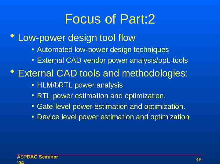
Focus of Part:2 Low-power design tool flow Automated low-power design techniques External CAD vendor power analysis/opt. tools External CAD tools and methodologies: HLM/bRTL power analysis RTL power estimation and optimization. Gate-level power estimation and optimization. Device level power estimation and optimization ASPDAC Seminar 46
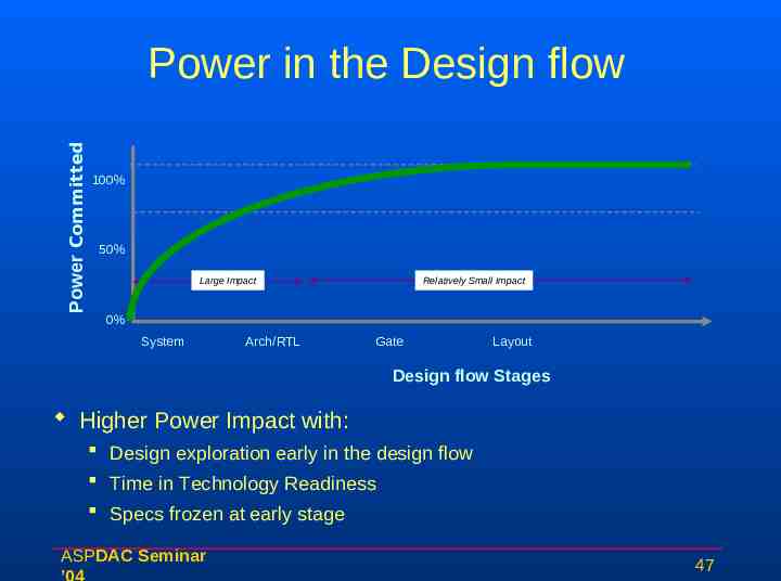
Power Committed Power in the Design flow 100% 50% Large Impact Relatively Small Impact 0% System Arch/RTL Gate Layout Design flow Stages Higher Power Impact with: Design exploration early in the design flow Time in Technology Readiness Specs frozen at early stage ASPDAC Seminar 47
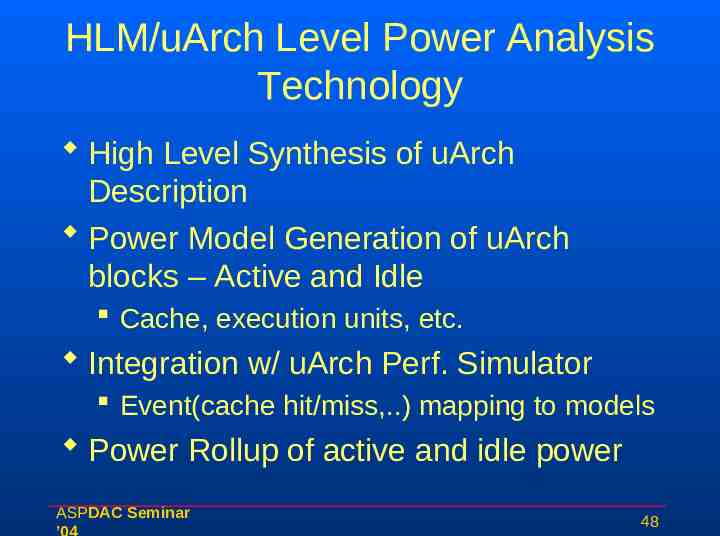
HLM/uArch Level Power Analysis Technology High Level Synthesis of uArch Description Power Model Generation of uArch blocks – Active and Idle Cache, execution units, etc. Integration w/ uArch Perf. Simulator Event(cache hit/miss,.) mapping to models Power Rollup of active and idle power ASPDAC Seminar 48
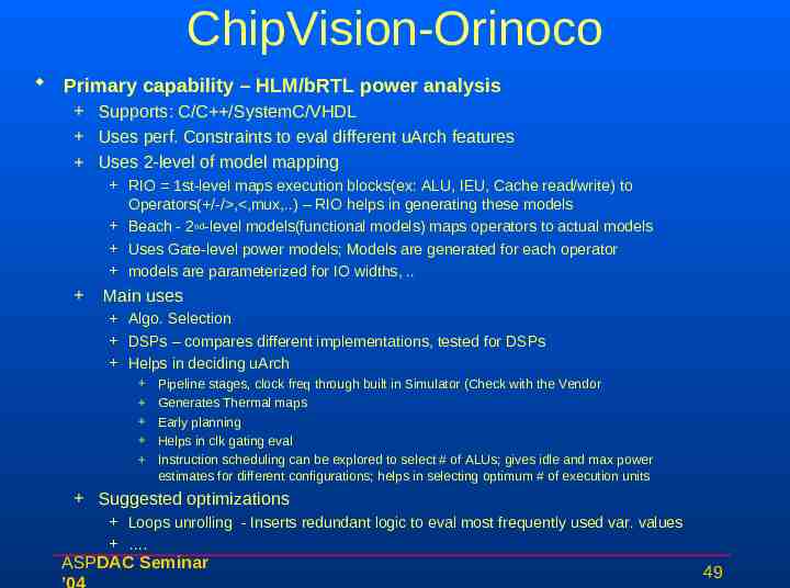
ChipVision-Orinoco Primary capability – HLM/bRTL power analysis Supports: C/C /SystemC/VHDL Uses perf. Constraints to eval different uArch features Uses 2-level of model mapping RIO 1st-level maps execution blocks(ex: ALU, IEU, Cache read/write) to Operators( /-/ , ,mux,.) – RIO helps in generating these models Beach - 2nd-level models(functional models) maps operators to actual models Uses Gate-level power models; Models are generated for each operator models are parameterized for IO widths, . Main uses Algo. Selection DSPs – compares different implementations, tested for DSPs Helps in deciding uArch Pipeline stages, clock freq through built in Simulator (Check with the Vendor Generates Thermal maps Early planning Helps in clk gating eval Instruction scheduling can be explored to select # of ALUs; gives idle and max power estimates for different configurations; helps in selecting optimum # of execution units Suggested optimizations Loops unrolling - Inserts redundant logic to eval most frequently used var. values . ASPDAC Seminar 49
ASC Primary Capability: RTL Simultaneous optimization of timing, power and area Maps HLM to RTL macros and writes out Verilog gate-level code, optimized for power bRTL optimizations for power Supports VHDL, Verilog bRTL Built-in simulation engine Analysis based on CDFG – control data flow graphs Performs high-level synthesis Roadmap: Support to C/Sys-C/Verilog planned ASPDAC Seminar 50
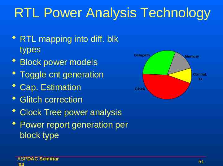
RTL Power Analysis Technology RTL mapping into diff. blk types Block power models Toggle cnt generation Cap. Estimation Glitch correction Clock Tree power analysis Power report generation per block type ASPDAC Seminar Datapath Memory Control, IO Clock 51
RTL Power Analysis Issues Toggle Count Generation Simulation model Simulator limitations – 0-delay, Unit-delay simulation Glitch accounting Early Capacitance data Estimated vs. extracted Changing floorplan, Wirecap estimation Design representation RLS/Custom Logic styles – ex: pass gate Mux/AND-OR mux Circuit Styles(Custom) – Domino vs. Static Clocks Clock-tree power Local clock-gating consideration Validation ASPDAC Seminar 52
Power Analysis goals and stimulus selection Power specing Typical, PowerVirus and idle applications Power grid design: Peak Power Power virus application – worst case power DECAP estimation, location and pwr/gnd noise: Idle to Max. power switching Two adjacent vectors that yield max difference Reliability - Electromigration, self heating Long running typical application Logic Simulation RTL vs. Gate Vector compaction preserves original vector characteristics improves runtime Gate-level AF propagation for Gate-level analysis Available in Power Compiler ’s gate-level analysis capability ASPDAC Seminar 53
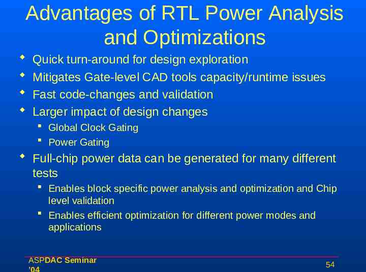
Advantages of RTL Power Analysis and Optimizations Quick turn-around for design exploration Mitigates Gate-level CAD tools capacity/runtime issues Fast code-changes and validation Larger impact of design changes Global Clock Gating Power Gating Full-chip power data can be generated for many different tests Enables block specific power analysis and optimization and Chip level validation Enables efficient optimization for different power modes and applications ASPDAC Seminar 54
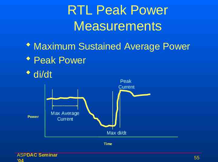
RTL Peak Power Measurements Maximum Sustained Average Power Peak Power di/dt Peak Current Power Max Average Current Max di/dt Time ASPDAC Seminar 55
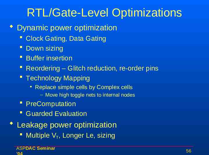
RTL/Gate-Level Optimizations Dynamic power optimization Clock Gating, Data Gating Down sizing Buffer insertion Reordering – Glitch reduction, re-order pins Technology Mapping Replace simple cells by Complex cells – Move high toggle nets to internal nodes PreComputation Guarded Evaluation Leakage power optimization Multiple VT, Longer Le, sizing ASPDAC Seminar 56
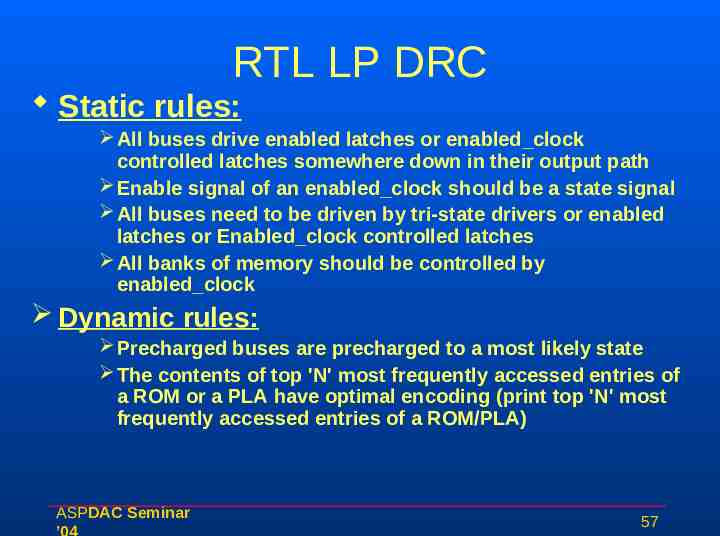
RTL LP DRC Static rules: All buses drive enabled latches or enabled clock controlled latches somewhere down in their output path Enable signal of an enabled clock should be a state signal All buses need to be driven by tri-state drivers or enabled latches or Enabled clock controlled latches All banks of memory should be controlled by enabled clock Dynamic rules: Precharged buses are precharged to a most likely state The contents of top 'N' most frequently accessed entries of a ROM or a PLA have optimal encoding (print top 'N' most frequently accessed entries of a ROM/PLA) ASPDAC Seminar 57
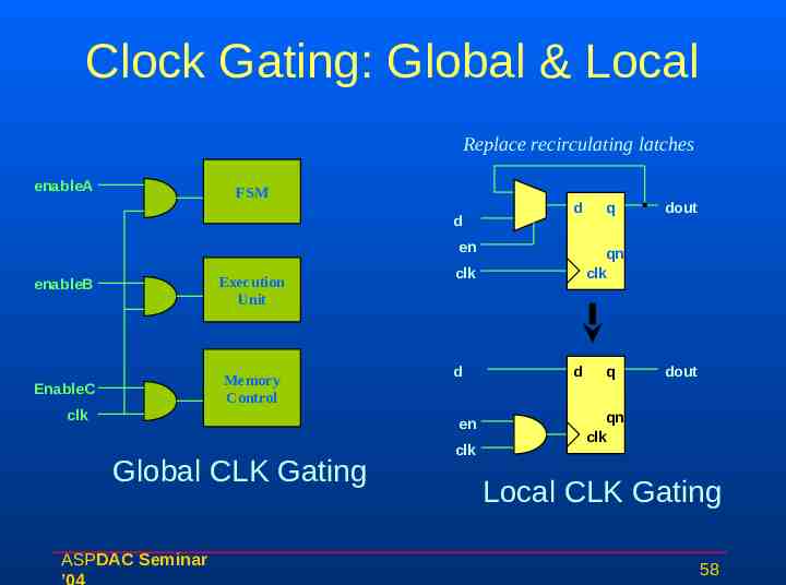
Clock Gating: Global & Local Replace recirculating latches enableA FSM d d en enableB Execution Unit EnableC Memory Control clk en Global CLK Gating ASPDAC Seminar clk dout qn clk clk d q d q dout qn clk Local CLK Gating 58
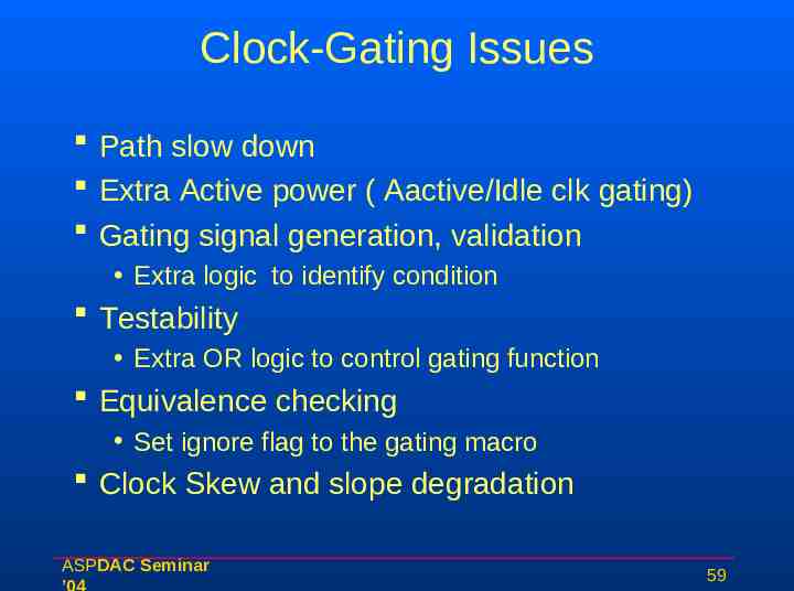
Clock-Gating Issues Path slow down Extra Active power ( Aactive/Idle clk gating) Gating signal generation, validation Extra logic to identify condition Testability Extra OR logic to control gating function Equivalence checking Set ignore flag to the gating macro Clock Skew and slope degradation ASPDAC Seminar 59
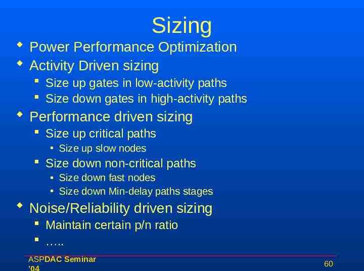
Sizing Power Performance Optimization Activity Driven sizing Size up gates in low-activity paths Size down gates in high-activity paths Performance driven sizing Size up critical paths Size up slow nodes Size down non-critical paths Size down fast nodes Size down Min-delay paths stages Noise/Reliability driven sizing Maintain certain p/n ratio . ASPDAC Seminar 60
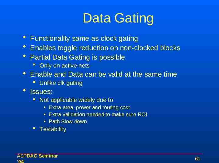
Data Gating Functionality same as clock gating Enables toggle reduction on non-clocked blocks Partial Data Gating is possible Only on active nets Enable and Data can be valid at the same time Unlike clk gating Issues: Not applicable widely due to Extra area, power and routing cost Extra validation needed to make sure ROI Path Slow down Testability ASPDAC Seminar 61
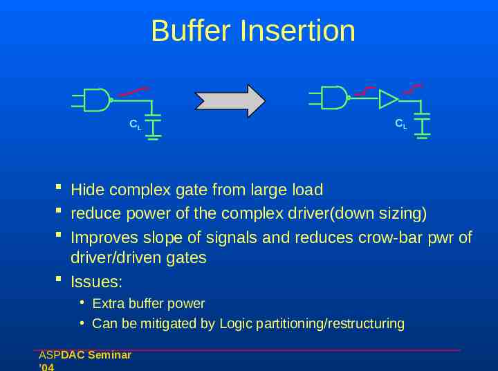
Buffer Insertion CL CL Hide complex gate from large load reduce power of the complex driver(down sizing) Improves slope of signals and reduces crow-bar pwr of driver/driven gates Issues: Extra buffer power Can be mitigated by Logic partitioning/restructuring ASPDAC Seminar
Synopsys - PowerTools PowerCompiler: RTL/Gate-level power analysis and optimization tool Accepts VCD/PLI to read the file VCD2SAIF – released Leakage trade-offs using dual-Vt handling Enhancements in RTL clock gating Link w/ Floorplanner Improved mem usage – 30% Test-logic insertion, clock tree insertion, placement and FV Selective clock gating Interface with SAIF, SPPM (Single Polynomial power model) support State dependent leakage models advised for accurate leakage est ROADMAP – runtime improvement Q3 ’02 AF propagation (RTL – to – Gate) PrimePower: Gate level average and instantaneous power analysis RTL and built-in simulation engine Other Similar tools: Sequence – PowerTheater, Cadence – BuildGates Extreme, ASPDAC Seminar 63
PrimePower (Synopsys) Capabilities/Key Features Gate level dynamic average and peak power verification/analysis Time-based power dissipation waveforms Uses gate-level simulation and precharacterized lib. power models for estimation Time based power waveform display w/ power hungry vectors Supports industry standard libraries Hierarchical navigation capability at the cell, block and full-chip level Capability to simulate complex gates, I/O pads and megacells Pros Accuracy: /-10% of SPICE (from data sheets) Good accuracy achieved by precise power modeling techniques (pattern dependent, partial voltage swing, etc), includes short-circuit and leakage power ASPDAC Seminar 64
Sequence - PowerTheater PowerTheater – RTL/Gate-level power analysis and optimization tool Includes 4 components: WattWatcher, WattSmith, VectorWatcher, PeakWatcher Replaced probabilistic AF propagation with 0 delay simulator IP Wizard for power model generation of IP blocks Vectorless power analysis WattSMITH: Wattbots , 18, for power opt., guidelines 2-level of modeling Verilog operators for high-level blocks- ALU, Cache, Regfiles Power models for ind. Operators Dual-Vt cell usage for leakage reduction Reads .lib and ALF models Uses “Showtime”(PrimeTime-SI) for post layout/postroute timing/power analysis Tightly coupled with Physical studio Platforms: Sun Solaris, HP UX. Memory: 512 MB minimum, 1GB recommended. Input formats: Verilog, VHDL, ALF vendor libraries, Synopsys Liberty (.lib) vendor libraries, OLA vendor libraries. Other Similar tools: Synposys – Power Compiler, PrimePower ASPDAC Seminar 65
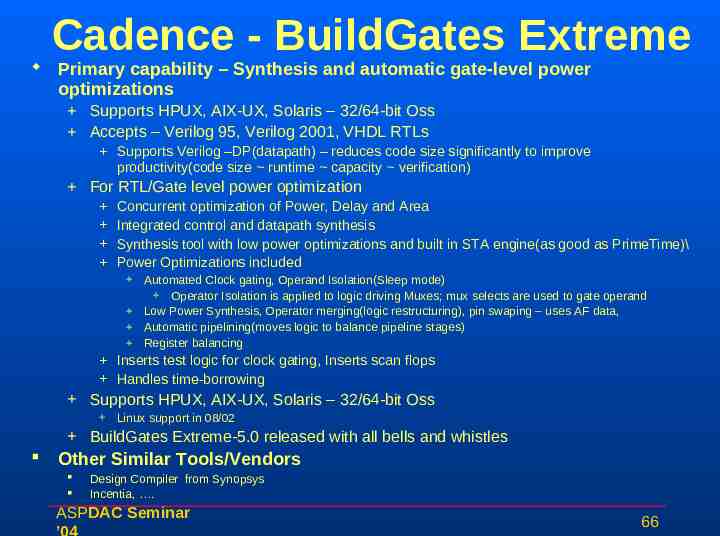
Cadence - BuildGates Extreme Primary capability – Synthesis and automatic gate-level power optimizations Supports HPUX, AIX-UX, Solaris – 32/64-bit Oss Accepts – Verilog 95, Verilog 2001, VHDL RTLs Supports Verilog –DP(datapath) – reduces code size significantly to improve productivity(code size runtime capacity verification) For RTL/Gate level power optimization Concurrent optimization of Power, Delay and Area Integrated control and datapath synthesis Synthesis tool with low power optimizations and built in STA engine(as good as PrimeTime)\ Power Optimizations included Automated Clock gating, Operand Isolation(Sleep mode) Operator Isolation is applied to logic driving Muxes; mux selects are used to gate operand Low Power Synthesis, Operator merging(logic restructuring), pin swaping – uses AF data, Automatic pipelining(moves logic to balance pipeline stages) Register balancing Inserts test logic for clock gating, Inserts scan flops Handles time-borrowing Supports HPUX, AIX-UX, Solaris – 32/64-bit Oss Linux support in 08/02 BuildGates Extreme-5.0 released with all bells and whistles Other Similar Tools/Vendors Design Compiler from Synopsys Incentia, . ASPDAC Seminar 66
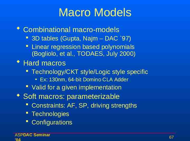
Macro Models Combinational macro-models 3D tables (Gupta, Najm – DAC 97) Linear regression based polynomials (Bogliolo, et al., TODAES, July 2000) Hard macros Technology/CKT style/Logic style specific Ex: 130nm, 64-bit Domino CLA Adder Valid for a given implementation Soft macros: parameterizable Constraints: AF, SP, driving strengths Technologies Configurations ASPDAC Seminar 67
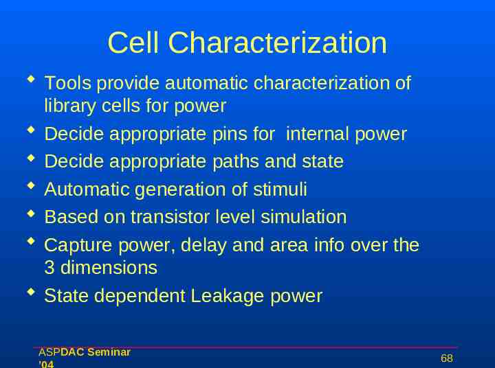
Cell Characterization Tools provide automatic characterization of library cells for power Decide appropriate pins for internal power Decide appropriate paths and state Automatic generation of stimuli Based on transistor level simulation Capture power, delay and area info over the 3 dimensions State dependent Leakage power ASPDAC Seminar 68
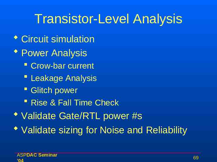
Transistor-Level Analysis Circuit simulation Power Analysis Crow-bar current Leakage Analysis Glitch power Rise & Fall Time Check Validate Gate/RTL power #s Validate sizing for Noise and Reliability ASPDAC Seminar 69
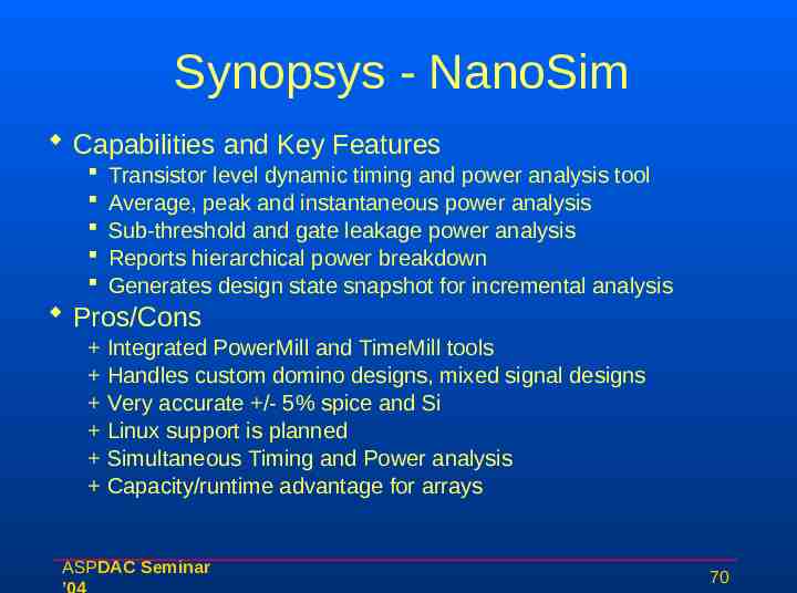
Synopsys - NanoSim Capabilities and Key Features Transistor level dynamic timing and power analysis tool Average, peak and instantaneous power analysis Sub-threshold and gate leakage power analysis Reports hierarchical power breakdown Generates design state snapshot for incremental analysis Pros/Cons Integrated PowerMill and TimeMill tools Handles custom domino designs, mixed signal designs Very accurate /- 5% spice and Si Linux support is planned Simultaneous Timing and Power analysis Capacity/runtime advantage for arrays ASPDAC Seminar 70
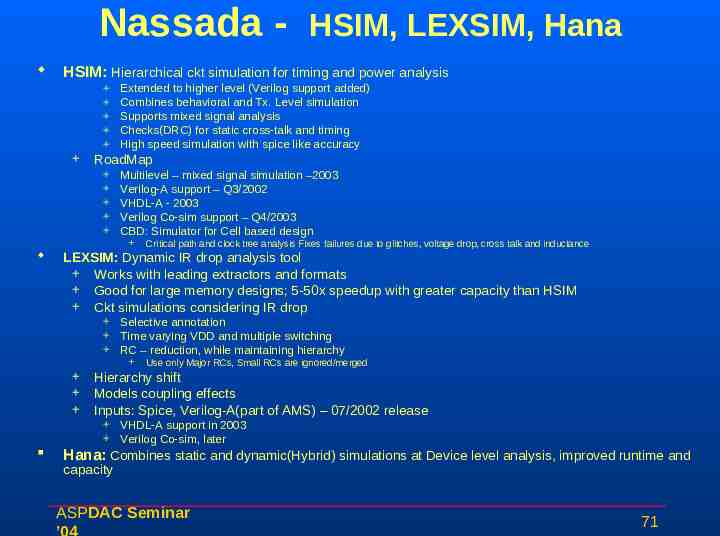
Nassada - HSIM, LEXSIM, Hana HSIM: Hierarchical ckt simulation for timing and power analysis Extended to higher level (Verilog support added) Combines behavioral and Tx. Level simulation Supports mixed signal analysis Checks(DRC) for static cross-talk and timing High speed simulation with spice like accuracy RoadMap Multilevel – mixed signal simulation –2003 Verilog-A support – Q3/2002 VHDL-A - 2003 Verilog Co-sim support – Q4/2003 CBD: Simulator for Cell based design Critical path and clock tree analysis Fixes failures due to glitches, voltage drop, cross talk and inductance LEXSIM: Dynamic IR drop analysis tool Works with leading extractors and formats Good for large memory designs; 5-50x speedup with greater capacity than HSIM Ckt simulations considering IR drop Selective annotation Time varying VDD and multiple switching RC – reduction, while maintaining hierarchy Use only Major RCs, Small RCs are ignored/merged Hierarchy shift Models coupling effects Inputs: Spice, Verilog-A(part of AMS) – 07/2002 release VHDL-A support in 2003 Verilog Co-sim, later Hana: Combines static and dynamic(Hybrid) simulations at Device level analysis, improved runtime and capacity ASPDAC Seminar 71
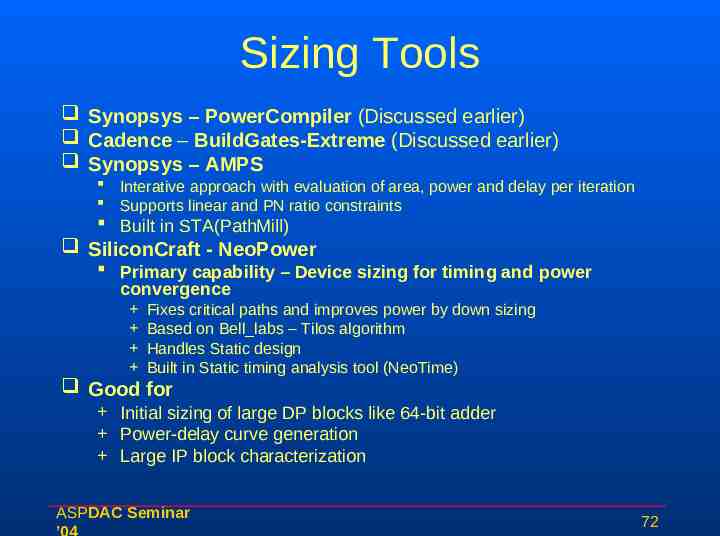
Sizing Tools Synopsys – PowerCompiler (Discussed earlier) Cadence – BuildGates-Extreme (Discussed earlier) Synopsys – AMPS Interative approach with evaluation of area, power and delay per iteration Supports linear and PN ratio constraints Built in STA(PathMill) SiliconCraft - NeoPower Primary capability – Device sizing for timing and power convergence Fixes critical paths and improves power by down sizing Based on Bell labs – Tilos algorithm Handles Static design Built in Static timing analysis tool (NeoTime) Good for Initial sizing of large DP blocks like 64-bit adder Power-delay curve generation Large IP block characterization ASPDAC Seminar 72
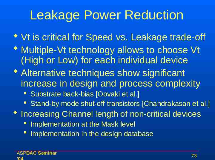
Leakage Power Reduction Vt is critical for Speed vs. Leakage trade-off Multiple-Vt technology allows to choose Vt (High or Low) for each individual device Alternative techniques show significant increase in design and process complexity Substrate back-bias [Oovaki et al.] Stand-by mode shut-off transistors [Chandrakasan et al.] Increasing Channel length of non-critical devices Implementation at the Mask level Implementation in the design database ASPDAC Seminar 73
Feature Summary of Other Power CAD tools ASPDAC Seminar 74
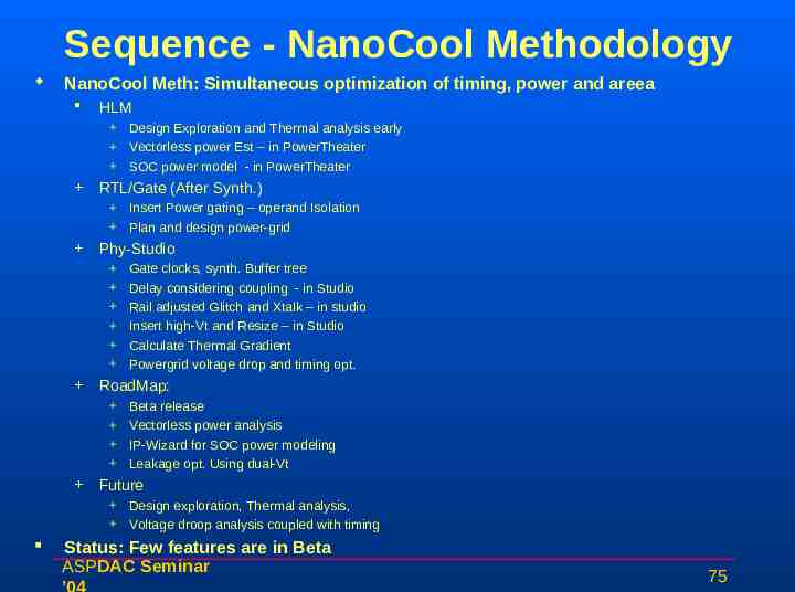
Sequence - NanoCool Methodology NanoCool Meth: Simultaneous optimization of timing, power and areea HLM Design Exploration and Thermal analysis early Vectorless power Est – in PowerTheater SOC power model - in PowerTheater RTL/Gate (After Synth.) Insert Power gating – operand Isolation Plan and design power-grid Phy-Studio RoadMap: Gate clocks, synth. Buffer tree Delay considering coupling - in Studio Rail adjusted Glitch and Xtalk – in studio Insert high-Vt and Resize – in Studio Calculate Thermal Gradient Powergrid voltage drop and timing opt. Beta release Vectorless power analysis IP-Wizard for SOC power modeling Leakage opt. Using dual-Vt Future Design exploration, Thermal analysis, Voltage droop analysis coupled with timing Status: Few features are in Beta ASPDAC Seminar 75
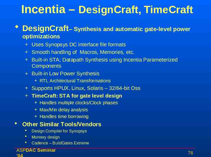
Incentia – DesignCraft, TimeCraft DesignCraft– Synthesis and automatic gate-level power optimizations Uses Synopsys DC interface file formats Smooth handling of Macros, Memories, etc. Built-in STA; Datapath Synthesis using Incentia Parameterized Components Built-in Low Power Synthesis RTL Architectural Transformations Supports HPUX, Linux, Solaris – 32/64-bit Oss TimeCraft: STA for gate level design Handles multiple clocks/Clock phases Max/Min delay analysis Handles time borrowing Other Similar Tools/Vendors Design Compiler for Synopsys Montery design Cadence – BuildGates Extreme ASPDAC Seminar 76
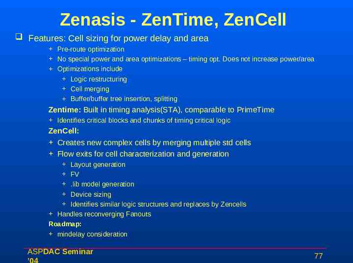
Zenasis - ZenTime, ZenCell Features: Cell sizing for power delay and area Pre-route optimization No special power and area optimizations – timing opt. Does not increase power/area Optimizations include Logic restructuring Cell merging Buffer/buffer tree insertion, splitting Zentime: Built in timing analysis(STA), comparable to PrimeTime Identifies critical blocks and chunks of timing critical logic ZenCell: Creates new complex cells by merging multiple std cells Flow exits for cell characterization and generation Layout generation FV .lib model generation Device sizing Identifies similar logic structures and replaces by Zencells Handles reconverging Fanouts Roadmap: mindelay consideration ASPDAC Seminar 77
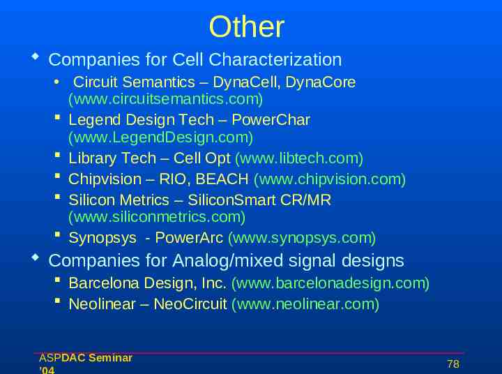
Other Companies for Cell Characterization Circuit Semantics – DynaCell, DynaCore (www.circuitsemantics.com) Legend Design Tech – PowerChar (www.LegendDesign.com) Library Tech – Cell Opt (www.libtech.com) Chipvision – RIO, BEACH (www.chipvision.com) Silicon Metrics – SiliconSmart CR/MR (www.siliconmetrics.com) Synopsys - PowerArc (www.synopsys.com) Companies for Analog/mixed signal designs Barcelona Design, Inc. (www.barcelonadesign.com) Neolinear – NeoCircuit (www.neolinear.com) ASPDAC Seminar 78
Conclusions Power is becoming more critical as we move to smaller geometries. Reliability issues are intensifying: IR drop, electromigration, EMI. Clock-gating is becoming ubiquitous. Multi-threshold adoption is increasing Speed vs. Leakage careful trade-off Multi-voltage designs are becoming a reality. Run Time Power Management is becoming mainstream at system level. ASPDAC Seminar 79
“Power CAD tools” Trends More CAD companies with new power CAD capabilities, across all design levels Many IP companies and foundries were stressing low power IP blocks and low leakage process support. CAD vendors are looking at power more closely to solve timing, RV and signal integrity issues Many mature tools from CAD vendors(Sequence, Nassda, Cadense, Simplex, OEA, ) to handle it. One major pwr CAD idea, where we are lagging, is multi-objective optimization at all design levels. ASPDAC Seminar 80
Q&A ASPDAC Seminar 81
Final Thoughts !! That’s all folks!!! ASPDAC Seminar 82
BACKUP ASPDAC Seminar 83
Drowsy Cache Design Blaauw et. al have shown that with simple architectural techniques, 80-90% of the non accessed cache lines can be maintained in a drowsy state affecting performance by 1-2 % only. During drowsy Vcc can be shut off State is not lost when power to unaccessed cache lines are shut off, there is area overhead with state retention which could be NON trivial For 65nm process technology generation, it is predicted that this technique would lower total power (standby and active) by 50-75 %. This is not verified by any actual design ASPDAC Seminar 84
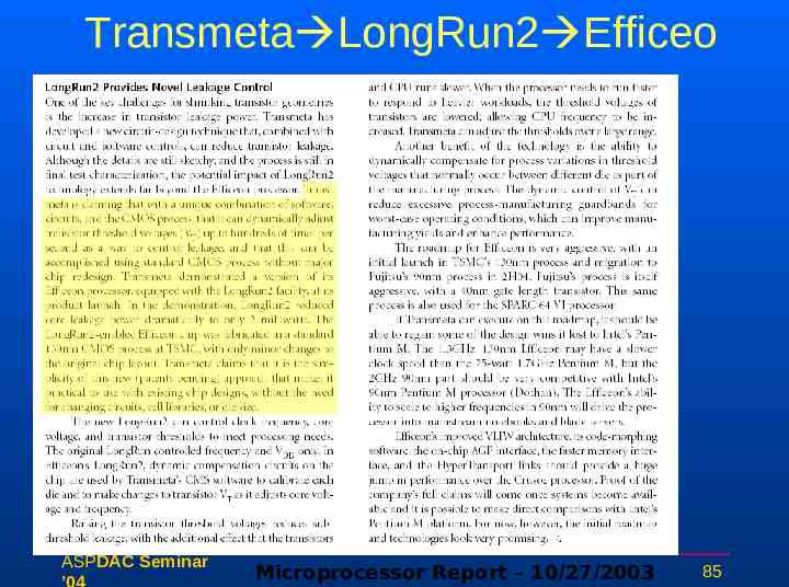
Transmeta LongRun2 Efficeo n ASPDAC Seminar Microprocessor Report – 10/27/2003 85
Cache Power Numbers from Published literature On-chip I and D (high speed SRAM) DEC 21164a (2.0Vdd, 0.35 , 400MHz, 30W max) I/D/L2 of 8/8/96KB and 1/1/3 associativity caches dissipate 25% of the total chip power DEC SA-110 (2.0Vdd, 0.35 , 233MHz, 1W typ) I/D of 16/16KB and 32/32 associativity (no L2 on-chip) I (D ) dissipate 27% (16%) of the total chip power Improving the power efficiency of caches is critical to the overall system power optimization ASPDAC Seminar 86
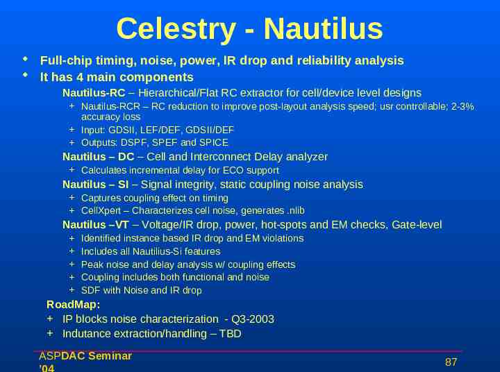
Celestry - Nautilus Full-chip timing, noise, power, IR drop and reliability analysis It has 4 main components Nautilus-RC – Hierarchical/Flat RC extractor for cell/device level designs Nautilus-RCR – RC reduction to improve post-layout analysis speed; usr controllable; 2-3% accuracy loss Input: GDSII, LEF/DEF, GDSII/DEF Outputs: DSPF, SPEF and SPICE Nautilus – DC – Cell and Interconnect Delay analyzer Calculates incremental delay for ECO support Nautilus – SI – Signal integrity, static coupling noise analysis Captures coupling effect on timing CellXpert – Characterizes cell noise, generates .nlib Nautilus –VT – Voltage/IR drop, power, hot-spots and EM checks, Gate-level Identified instance based IR drop and EM violations Includes all Nautilius-Si features Peak noise and delay analysis w/ coupling effects Coupling includes both functional and noise SDF with Noise and IR drop RoadMap: IP blocks noise characterization - Q3-2003 Indutance extraction/handling – TBD ASPDAC Seminar 87
