ISO 10110 Optical Drawing Standards Introduction to
17 Slides578.72 KB
ISO 10110 Optical Drawing Standards Introduction to Opto-Mechanical Engineering OPTI 521 University of Arizona, College of Optical Sciences Jason Lane 13 December 2009
ISO 10110 What is it? ISO standard describing preparation of drawings for optical elements and systems Describes features unique to optical components – builds on GD&T standards (compatible with ASME Y14.5M) ISO version of ASME Y14.18M (which will likely be superseded by ISO 10110 or some equivalent). Who uses it? Almost all of the optical design / manufacturing industry. Both internationally and in the U.S. All of the major optical design packages output ISO 10110 compliant element drawings. Why do we care? GD&T alone will not help you interpret an optical element or system drawing. ISO 10110 is essential, and ISO compliant drawings will be encountered 99.99% of the time. For example . 2
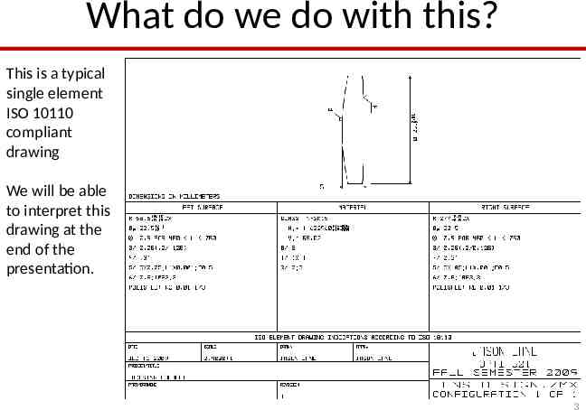
What do we do with this? This is a typical single element ISO 10110 compliant drawing We will be able to interpret this drawing at the end of the presentation. 3
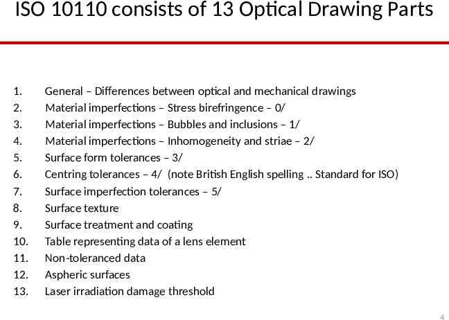
ISO 10110 consists of 13 Optical Drawing Parts 1. 2. 3. 4. 5. 6. 7. 8. 9. 10. 11. 12. 13. General – Differences between optical and mechanical drawings Material imperfections – Stress birefringence – 0/ Material imperfections – Bubbles and inclusions – 1/ Material imperfections – Inhomogeneity and striae – 2/ Surface form tolerances – 3/ Centring tolerances – 4/ (note British English spelling . Standard for ISO) Surface imperfection tolerances – 5/ Surface texture Surface treatment and coating Table representing data of a lens element Non-toleranced data Aspheric surfaces Laser irradiation damage threshold 4
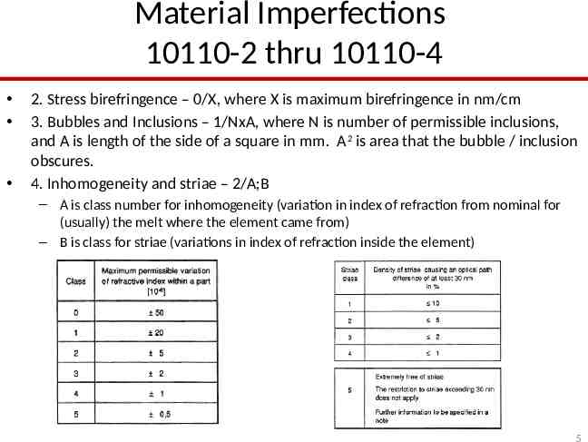
Material Imperfections 10110-2 thru 10110-4 2. Stress birefringence – 0/X, where X is maximum birefringence in nm/cm 3. Bubbles and Inclusions – 1/NxA, where N is number of permissible inclusions, and A is length of the side of a square in mm. A 2 is area that the bubble / inclusion obscures. 4. Inhomogeneity and striae – 2/A;B – A is class number for inhomogeneity (variation in index of refraction from nominal for (usually) the melt where the element came from) – B is class for striae (variations in index of refraction inside the element) 5
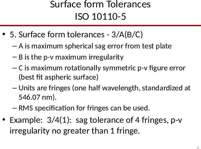
Surface form Tolerances ISO 10110-5 5. Surface form tolerances - 3/A(B/C) – A is maximum spherical sag error from test plate – B is the p-v maximum irregularity – C is maximum rotationally symmetric p-v figure error (best fit aspheric surface) – Units are fringes (one half wavelength, standardized at 546.07 nm). – RMS specification for fringes can be used. Example: 3/4(1): sag tolerance of 4 fringes, p-v irregularity no greater than 1 fringe. 6
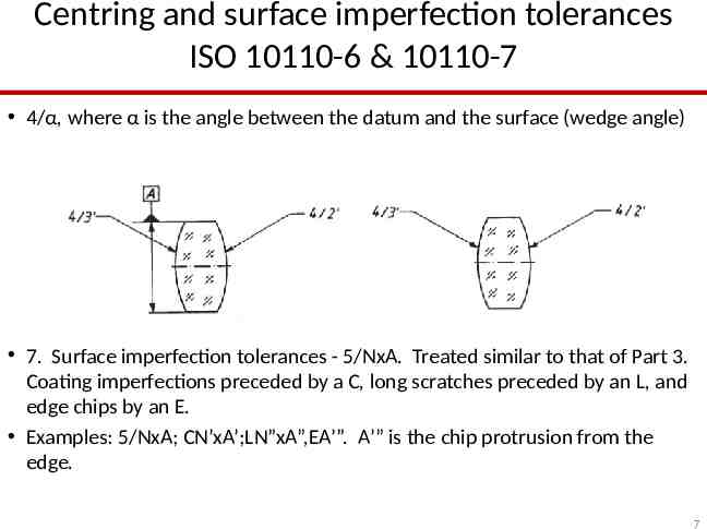
Centring and surface imperfection tolerances ISO 10110-6 & 10110-7 4/α, where α is the angle between the datum and the surface (wedge angle) 7. Surface imperfection tolerances - 5/NxA. Treated similar to that of Part 3. Coating imperfections preceded by a C, long scratches preceded by an L, and edge chips by an E. Examples: 5/NxA; CN’xA’;LN”xA”,EA’”. A’” is the chip protrusion from the edge. 7
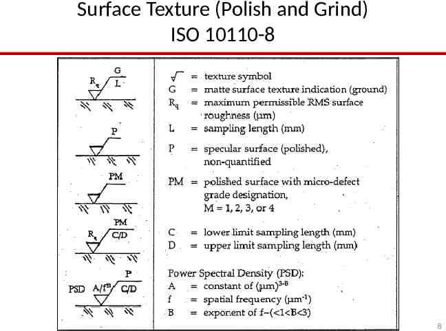
Surface Texture (Polish and Grind) ISO 10110-8 8
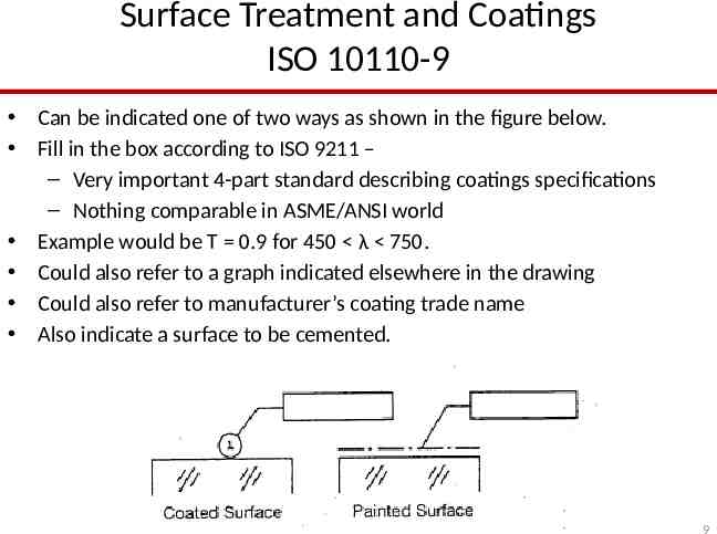
Surface Treatment and Coatings ISO 10110-9 Can be indicated one of two ways as shown in the figure below. Fill in the box according to ISO 9211 – – Very important 4-part standard describing coatings specifications – Nothing comparable in ASME/ANSI world Example would be T 0.9 for 450 λ 750. Could also refer to a graph indicated elsewhere in the drawing Could also refer to manufacturer’s coating trade name Also indicate a surface to be cemented. 9
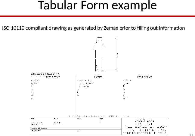
Compiling data in tabular form ISO 10110-10 Can become cluttered for simple element drawings. Tabular form provides simpler method of presenting information to avoid ambiguity and errors in reading Major optical design programs have adopted presenting ISO 10110 data in tabular form – ZEMAX - used by Navy – Code V - used by Raytheon (among others) This will be most common drawing form encountered 10
Tabular Form example ISO 10110 compliant drawing as generated by Zemax prior to filling out information 11
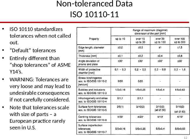
Non-toleranced Data ISO 10110-11 ISO 10110 standardizes tolerances when not called out. “Default” tolerances Entirely different than “shop tolerances” of ASME Y14’s. WARNING: Tolerances are very loose and may lead to undesirable consequences if not carefully considered. Note that tolerances scale with size of parts – a European practice rarely seen in U.S. 12
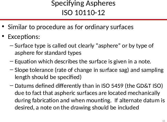
Specifying Aspheres ISO 10110-12 Similar to procedure as for ordinary surfaces Exceptions: – Surface type is called out clearly “asphere” or by type of asphere for standard types – Equation which describes the surface is given in a note. – Slope tolerance (rate of change in surface sag) and sampling length should be specified) – Datums defined differently than in ISO 5459 (the GD&T ISO) due to fact that aspheric surfaces are located mechanically during fabrication and when mounting. If alternate datum is desired, a note on the drawing should be included 13
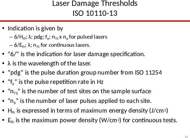
Laser Damage Thresholds ISO 10110-13 Indication is given by – 6/Hth; λ; pdg; fp; nTS x np for pulsed lasers – 6/Eth; λ; nTS for continuous lasers. “6/” is the indication for laser damage specification. λ is the wavelength of the laser. “pdg” is the pulse duration group number from ISO 11254 “fp” is the pulse repetition rate in Hz “nTS” is the number of test sites on the sample surface “np” is the number of laser pulses applied to each site. Hth is expressed in terms of maximum energy density (J/cm 2) Eth is the maximum power density (W/cm2) for continuous tests. 14
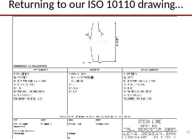
Returning to our ISO 10110 drawing 15
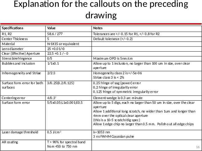
Explanation for the callouts on the preceding drawing Specifications Value Notes R1, R2 Center Thickness Material Lens diameter Clear (Effective) Aperture Stress birefringence Bubbles and inclusion 58.6 / 277 5 N-SK15 or equivalent 25 0.01/-0 22.5 0.1 / - 0 0/5 1/1x0.1 Tolerances are /- 0.15 for R1, /- 0.8 for R2 Default tolerance ( /- 0.2) Inhomogeneity and Striae 2/2:3 Surface form error for both surfaces 3/0.25(0.2/0.125) Centering error Surface form error 4/0.3’ 5/5x0.05;L1x0.001;E0.5 Element wedge is 0.3 arc minute Allow up to 5 digs, each no larger than 50 um in size, over the clear aperture Allow 1 additional long scratch, no wider than 1um and longer than 4mm over the optical clear aperture (this is a 10-5 scratch/dig spec) Allow 1 edge chip no larger than 0.5 mm. Polish out all edge chips Laser damage threshold 0.5 J/cm2 λ 1053 nm 3 ns FWHM Gaussian pulse AR coating T 90% for spectral band from 450 to 750 nm Maximum OPD is 5nm/cm Allow up to 1 inclusion, no larger than 100 um in size, over clear aperture Homogeneity class 2 is /-5e-06 Striae class 3 is 2% 0.25 fringe of sag (power) error 0.2 fringe of irregularity error 0.125 fringe of symmetric irregularity error 16
References for further information Tutorial on ISO 10110 Optical Drawing Standards, Jason Lane. Tutorial white paper which accompanies this presentation (lists all the ISO standards relating to optics and optical systems). See me for copy. ISO 10110 Optics and Optical Instruments – Preparation of drawings for optical elements and systems: A User’s Guide by Ronald K. Kimmel and Robert E. Parks The ISO 10110 standards themselves (and ISO 9211) SPIE regularly hosts ISO 10110 short courses taught by David M. Aikens. Available on spie.org website 17
