Hardware & Firmware work in the UK In the UK we are focused on
30 Slides5.14 MB
Hardware & Firmware work in the UK In the UK we are focused on the phase 1& phase 2 upgrades. CPM High-Speed demonstrator Multi-Gbps PCB simulation 05/07/2024 Weiming Qian On behalf of UK 1
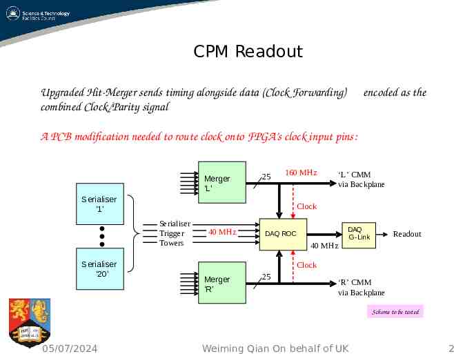
CPM Readout Upgraded Hit-Merger sends timing alongside data (Clock Forwarding) combined Clock/Parity signal encoded as the A PCB modification needed to route clock onto FPGA’s clock input pins: Merger ‘L’ 25 Serialiser ‘1’ ‘L’ CMM via Backplane Clock Serialiser Trigger Towers Serialiser ‘20’ 160 MHz 40 MHz DAQ ROC 40 MHz DAQ G-Link Readout Clock Merger ‘R’ 25 ‘R’ CMM via Backplane Scheme to be tested 05/07/2024 Weiming Qian On behalf of UK 2
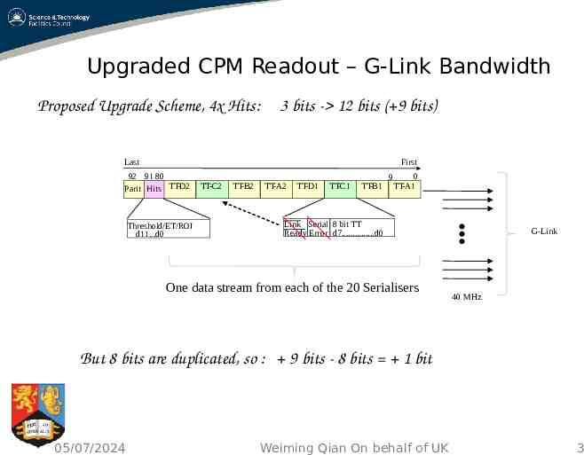
Upgraded CPM Readout – G-Link Bandwidth Proposed Upgrade Scheme, 4x Hits: 3 bits - 12 bits ( 9 bits) Last First 92 91 80 Parit Hits TT-D2 y Threshold/ET/ROI d11.d0 TT-C2 TT-B2 TT-A2 TT-D1 TT-C1 TT-B1 0 9 TT-A1 Link Serial 8 bit TT Ready Error d7.d0 data One data stream from each of the 20 Serialisers G-Link 40 MHz But 8 bits are duplicated, so : 9 bits - 8 bits 1 bit 05/07/2024 Weiming Qian On behalf of UK 3
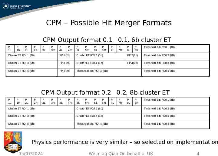
CPM – Possible Hit Merger Formats CPM Output format 0.1 0.1, 6b cluster ET P 1L P 1R P 2L P 2R P 3L P 3R P 4L P 4R P 5L P 5R P 6L P 6R P 7L P 7R P 8L P 8R Threshold bits ROI 1 (8B) Cluster ET ROI 1 (6b) FP 1(2b) Cluster ET ROI 2 (6b) FP 2(2b) Threshold bits ROI 2 (8B) Cluster ET ROI 3 (6b) FP 3(2b) Cluster ET ROI 4 (6b) FP 4(2b) Threshold bits ROI 3 (8B) Cluster ET ROI 5 (6b) FP 5(2b) Threshold bits ROI 4 (8B) Threshold bits ROI 5 (8B) CPM Output format 0.2 0.2, 8b cluster ET P 1L P 1R P 2L P 2R P 3L P 3R P 4L P 4R P 5L P 5R P 6L P 6R P 7L P 7R P 8L P 8R Threshold bits ROI 1 (8B) Cluster ET ROI 1 (8b) Cluster ET ROI 2 (8b) Threshold bits ROI 2 (8B) Cluster ET ROI 3 (8b) Cluster ET ROI 4 (8b) Threshold bits ROI 3 (8B) Cluster ET ROI 5 (8b) Threshold bits ROI 4 (8B) Threshold bits ROI 5 (8B) Physics performance is very similar – so selected on implementation 05/07/2024 Weiming Qian On behalf of UK 4
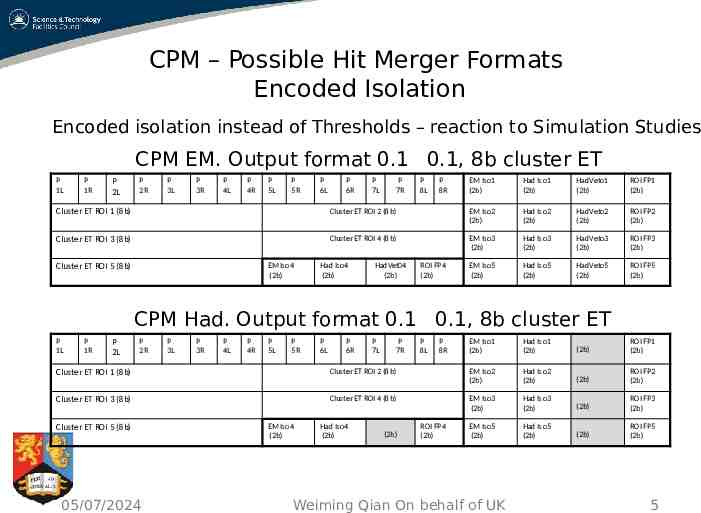
CPM – Possible Hit Merger Formats Encoded Isolation Encoded isolation instead of Thresholds – reaction to Simulation Studies CPM EM. Output format 0.1 0.1, 8b cluster ET P 1L P 1R P 2L P 2R P 3L P 3R P 4L P 4R P 5L P 5R P 6L P 6R P 7L P 7R P 8L P 8R EM Iso1 (2b) Had Iso1 (2b) HadVeto1 (2b) ROI FP1 (2b) Cluster ET ROI 1 (8b) Cluster ET ROI 2 (8b) EM Iso2 (2b) Had Iso2 (2b) HadVeto2 (2b) ROI FP2 (2b) Cluster ET ROI 3 (8b) Cluster ET ROI 4 (8b) EM Iso3 (2b) Had Iso3 (2b) HadVeto3 (2b) ROI FP3 (2b) EM Iso5 (2b) Had Iso5 (2b) HadVeto5 (2b) ROI FP5 (2b) EM Iso4 (2b) Cluster ET ROI 5 (8b) Had Iso4 (2b) HadVet04 (2b) ROI FP4 (2b) CPM Had. Output format 0.1 0.1, 8b cluster ET P 1L P 1R P 2L P 2R P 3L P 3R P 4L P 4R P 5L P 5R P 6L P 6R P 7L P 7R Cluster ET ROI 1 (8b) Cluster ET ROI 2 (8b) Cluster ET ROI 3 (8b) Cluster ET ROI 4 (8b) Cluster ET ROI 5 (8b) 05/07/2024 EM Iso4 (2b) Had Iso4 (2b) (2b) P 8L P 8R ROI FP4 (2b) EM Iso1 (2b) Had Iso1 (2b) (2b) ROI FP1 (2b) EM Iso2 (2b) Had Iso2 (2b) (2b) ROI FP2 (2b) EM Iso3 (2b) Had Iso3 (2b) (2b) ROI FP3 (2b) EM Iso5 (2b) Had Iso5 (2b) (2b) ROI FP5 (2b) Weiming Qian On behalf of UK 5
CPM Firmware Preparing design environment for developing firmware in Ph1. Moving projects from Mentor HDL Designer to Xilinx ISE 10.1: Tidy-up designs. Revision. Better Test-Benches (ModSim). Hit-Merger New project created in ISE DAQ G-Link Readout Moved – checking files/libs ROI G-Link Readout To do CP Chip 05/07/2024 To do Weiming Qian On behalf of UK 6
CPM Firmware Timescales Hope to produce code for FPGAs using just ISE (with same functionality as current designs) by the end of 2011. Compare behaviour of new code with current version: Deep Simulation B’ham Testrig - CERN Point 1 ? Have FPGAs debugged & ready for early 2012 cosmics running If time, add new threshold-ing scheme to CP FPGA also. Isolation & energy thresholds combined, say EM16I and EM20 - one hit. Aim to have Phase1 upgrade designs ready by end of 2013 for big shutdown. 05/07/2024 Weiming Qian On behalf of UK 7
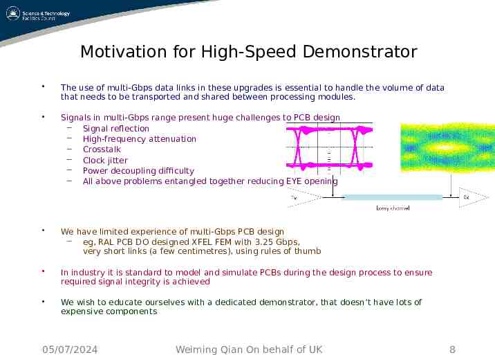
Motivation for High-Speed Demonstrator The use of multi-Gbps data links in these upgrades is essential to handle the volume of data that needs to be transported and shared between processing modules. Signals in multi-Gbps range present huge challenges to PCB design – Signal reflection – High-frequency attenuation – Crosstalk – Clock jitter – Power decoupling difficulty – All above problems entangled together reducing EYE opening We have limited experience of multi-Gbps PCB design – eg, RAL PCB DO designed XFEL FEM with 3.25 Gbps, very short links (a few centimetres), using rules of thumb In industry it is standard to model and simulate PCBs during the design process to ensure required signal integrity is achieved We wish to educate ourselves with a dedicated demonstrator, that doesn’t have lots of expensive components 05/07/2024 Weiming Qian On behalf of UK 8
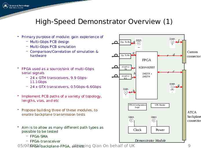
High-Speed Demonstrator Overview (1) Primary purpose of module: gain experience of – Multi-Gbps PCB design – Multi-Gbps PCB simulation – Comparison/Correlation of simulation & hardware Op. Tx/Rx Op. Tx/Rx f e a Custom connector d FPGA FPGA used as a source/sink of multi-Gbps serial signals – 24 x GTH transceivers, 9.9 Gbps– 11.1Gbps – 24 x GTX transceivers, 0.5Gbps–6.6Gbps SNAP 12 TX SNAP 12 RX XC6VHX255T h c 24GTX 24GTH g b Implement PCB paths of a variety of topology, lengths, vias, and etc Propose building three of these modules, to enable backplane transmission tests FPGA Configuration Logic CPU Header Aim is to allow as many different path types as Clock Power possible to be tested – FPGA-SMA Demonstrator Module – FPGA–transceiver – FPGA–backplane–FPGA, and 05/07/2024 Weiming Qian On behalf of UK etc ATCA backplane connector 9
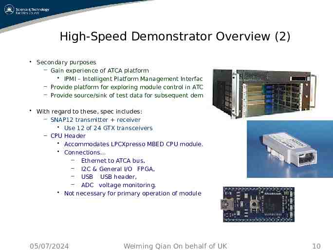
High-Speed Demonstrator Overview (2) Secondary purposes – Gain experience of ATCA platform IPMI – Intelligent Platform Management Interface – Provide platform for exploring module control in ATCA (e.g. Ethernet) – Provide source/sink of test data for subsequent demonstrator modules With regard to these, spec includes: – SNAP12 transmitter receiver Use 12 of 24 GTX transceivers – CPU Header Accommodates LPCXpresso MBED CPU module. Connections – Ethernet to ATCA bus, – I2C & General I/O FPGA, – USB USB header, – ADC voltage monitoring. Not necessary for primary operation of module 05/07/2024 Weiming Qian On behalf of UK 10
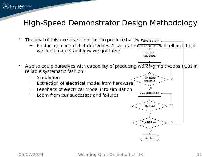
High-Speed Demonstrator Design Methodology The goal of this exercise is not just to produce hardware – Producing a board that does/doesn't work at multi-Gbps will tell us little if we don't understand how we got there. Also to equip ourselves with capability of producing working multi-Gbps PCBs in reliable systematic fashion: – Simulation – Extraction of electrical model from hardware – Feedback of electrical model into simulation – Learn from our successes and failures 05/07/2024 Weiming Qian On behalf of UK 11
High-Speed Demonstrator Status Conceptual design review held June 2011 – documents available at https://indico.cern.ch/event/HSDReview110615 Schematic entry underway Currently designing ATCA Power system – ATCA: board negotiates with shelf controller for power supply & backplane access – High Speed Demonstrator hardware capable of implementing full ATCA specification Spartan FPGA used as board power management controller (IPMC) Based on XFEL Train Builder board (RAL) – Manual over-ride enables quick commissioning of other aspects of board On schedule for manufacture beginning of next year 05/07/2024 Weiming Qian On behalf of UK 12
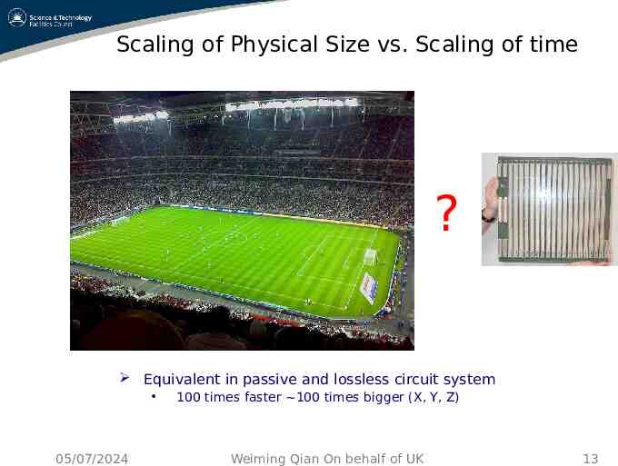
Scaling of Physical Size vs. Scaling of time ? Equivalent in passive and lossless circuit system 05/07/2024 100 times faster 100 times bigger (X, Y, Z) Weiming Qian On behalf of UK 13
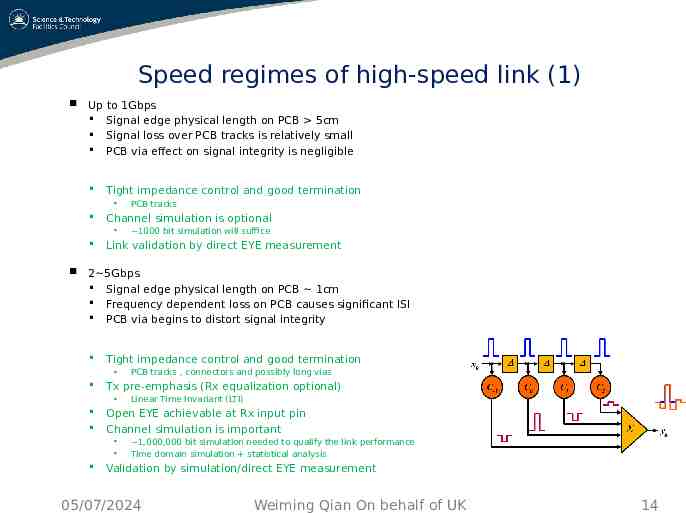
Speed regimes of high-speed link (1) Up to 1Gbps Signal edge physical length on PCB 5cm Signal loss over PCB tracks is relatively small PCB via effect on signal integrity is negligible Tight impedance control and good termination Channel simulation is optional PCB tracks 1000 bit simulation will suffice Link validation by direct EYE measurement 2 5Gbps Signal edge physical length on PCB 1cm Frequency dependent loss on PCB causes significant ISI PCB via begins to distort signal integrity Tight impedance control and good termination Tx pre-emphasis (Rx equalization optional) Linear Time Invariant (LTI) Open EYE achievable at Rx input pin Channel simulation is important PCB tracks , connectors and possibly long vias 1,000,000 bit simulation needed to qualify the link performance Time domain simulation statistical analysis Validation by simulation/direct EYE measurement 05/07/2024 Weiming Qian On behalf of UK 14
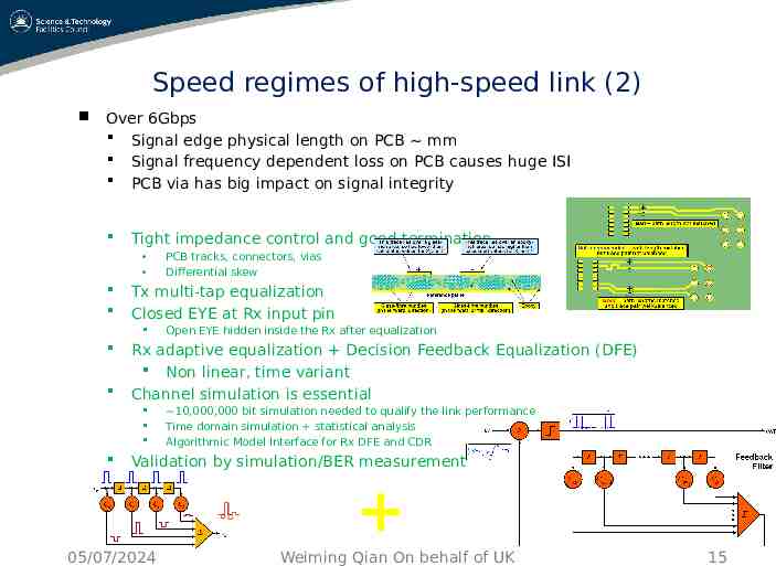
Speed regimes of high-speed link (2) Over 6Gbps Signal edge physical length on PCB mm Signal frequency dependent loss on PCB causes huge ISI PCB via has big impact on signal integrity Tight impedance control and good termination Tx multi-tap equalization Closed EYE at Rx input pin Open EYE hidden inside the Rx after equalization Rx adaptive equalization Decision Feedback Equalization (DFE) Non linear, time variant Channel simulation is essential PCB tracks, connectors, vias Differential skew 10,000,000 bit simulation needed to qualify the link performance Time domain simulation statistical analysis Algorithmic Model Interface for Rx DFE and CDR Validation by simulation/BER measurement 05/07/2024 Weiming Qian On behalf of UK 15
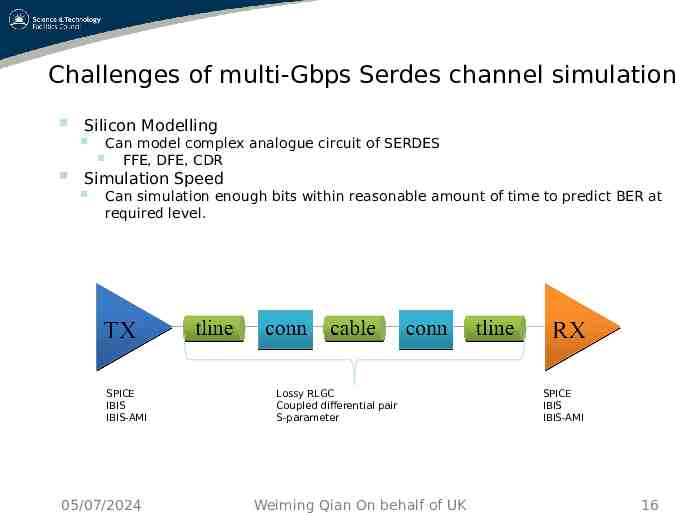
Challenges of multi-Gbps Serdes channel simulation Silicon Modelling Can model complex analogue circuit of SERDES FFE, DFE, CDR Simulation Speed Can simulation enough bits within reasonable amount of time to predict BER at required level. SPICE IBIS IBIS-AMI 05/07/2024 Lossy RLGC Coupled differential pair S-parameter Weiming Qian On behalf of UK SPICE IBIS IBIS-AMI 16
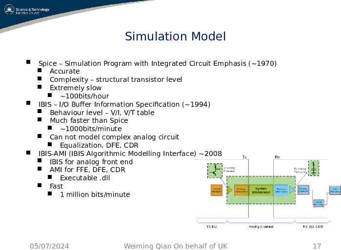
Simulation Model Spice – Simulation Program with Integrated Circuit Emphasis ( 1970) Accurate Complexity – structural transistor level Extremely slow 100bits/hour IBIS – I/O Buffer Information Specification ( 1994) Behaviour level – V/I, V/T table Much faster than Spice 1000bits/minute Can not model complex analog circuit Equalization, DFE, CDR IBIS-AMI (IBIS Algorithmic Modelling Interface) 2008 IBIS for analog front end AMI for FFE, DFE, CDR Executable .dll Fast 1 million bits/minute 05/07/2024 Weiming Qian On behalf of UK 17
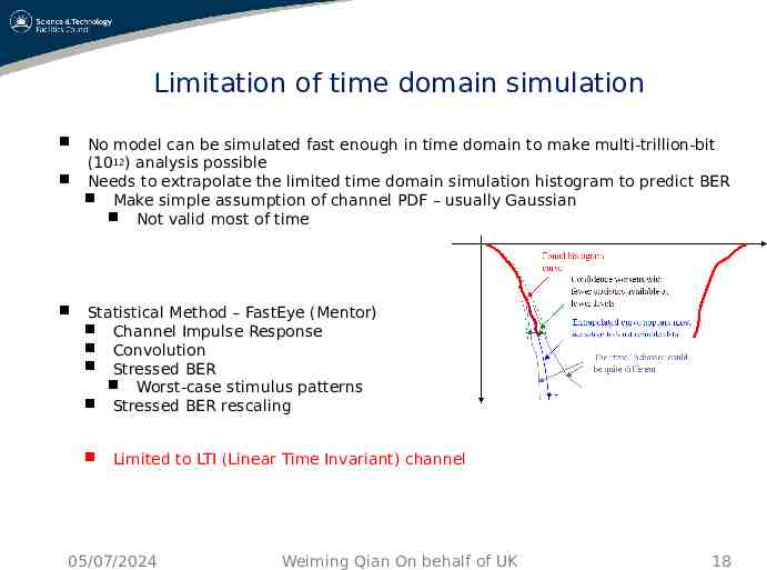
Limitation of time domain simulation No model can be simulated fast enough in time domain to make multi-trillion-bit (1012) analysis possible Needs to extrapolate the limited time domain simulation histogram to predict BER Make simple assumption of channel PDF – usually Gaussian Not valid most of time Statistical Method – FastEye (Mentor) Channel Impulse Response Convolution Stressed BER Worst-case stimulus patterns Stressed BER rescaling Limited to LTI (Linear Time Invariant) channel 05/07/2024 Weiming Qian On behalf of UK 18
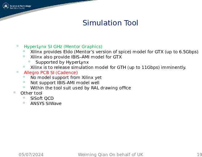
Simulation Tool HyperLynx SI GHz (Mentor Graphics) Xilinx provides Eldo (Mentor’s version of spice) model for GTX (up to 6.5Gbps) Xilinx also provide IBIS–AMI model for GTX Supported by HyperLynx Xilinx is to release simulation model for GTH (up to 11Gbps) imminently. Allegro PCB SI (Cadence) No model support from Xilinx yet Not support IBIS-AMI model well Within the tool suit used by RAL drawing office Other tool SiSoft QCD ANSYS SIWave 05/07/2024 Weiming Qian On behalf of UK 19
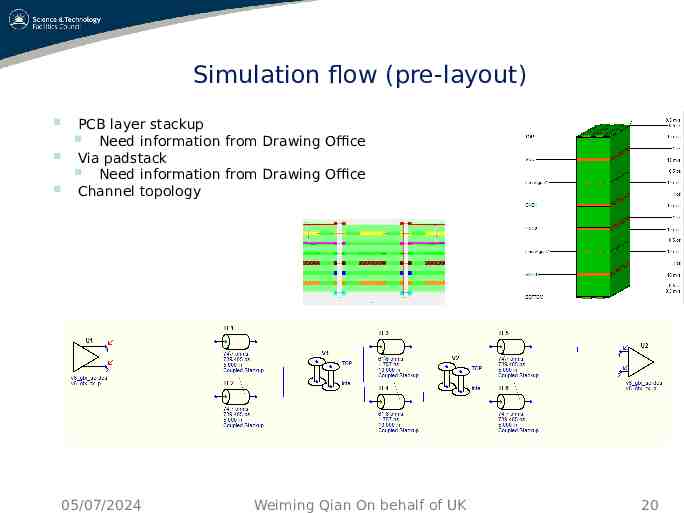
Simulation flow (pre-layout) PCB layer stackup Need information from Drawing Office Via padstack Need information from Drawing Office Channel topology 05/07/2024 Weiming Qian On behalf of UK 20
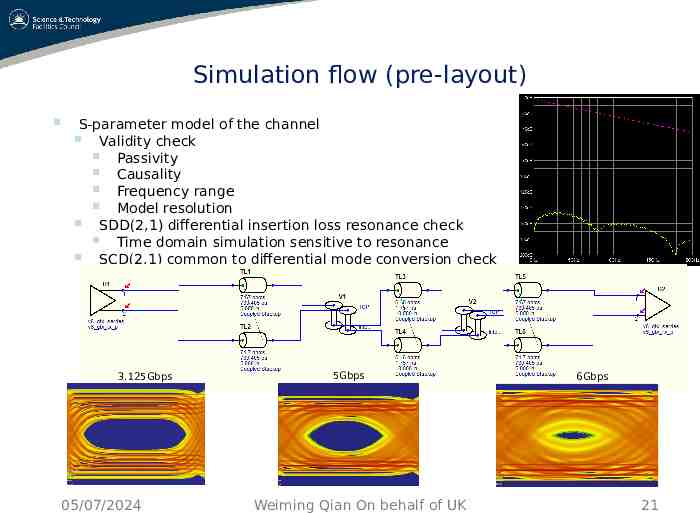
Simulation flow (pre-layout) S-parameter model of the channel Validity check Passivity Causality Frequency range Model resolution SDD(2,1) differential insertion loss resonance check Time domain simulation sensitive to resonance SCD(2,1) common to differential mode conversion check 3.125Gbps 05/07/2024 5Gbps Weiming Qian On behalf of UK 6Gbps 21
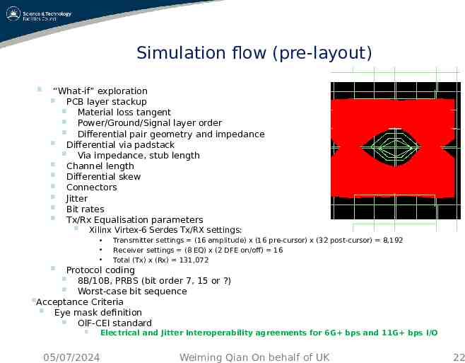
Simulation flow (pre-layout) “What-if” exploration PCB layer stackup Material loss tangent Power/Ground/Signal layer order Differential pair geometry and impedance Differential via padstack Via impedance, stub length Channel length Differential skew Connectors Jitter Bit rates Tx/Rx Equalisation parameters Xilinx Virtex-6 Serdes Tx/RX settings: Transmitter settings (16 amplitude) x (16 pre-cursor) x (32 post-cursor) 8,192 Receiver settings (8 EQ) x (2 DFE on/off) 16 Total (Tx) x (Rx) 131,072 Protocol coding 8B/10B, PRBS (bit order 7, 15 or ?) Worst-case bit sequence Acceptance Criteria Eye mask definition OIF-CEI standard 05/07/2024 Electrical and Jitter Interoperability agreements for 6G bps and 11G bps I/O Weiming Qian On behalf of UK 22
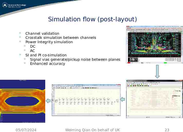
Simulation flow (post-layout) Channel validation Crosstalk simulation between channels Power Integrity simulation DC AC SI and PI co-simulation Signal vias generate/pickup noise between planes Enhanced accuracy 05/07/2024 Weiming Qian On behalf of UK 23
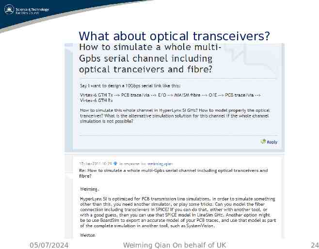
What about optical transceivers? 05/07/2024 Weiming Qian On behalf of UK 24
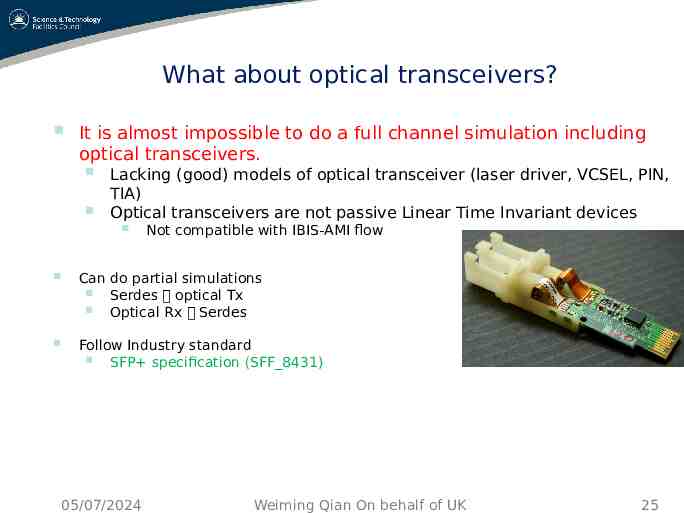
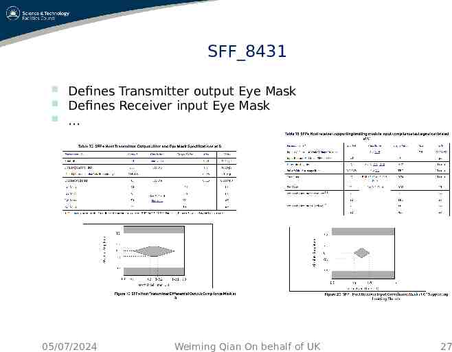
What about optical transceivers? It is almost impossible to do a full channel simulation including optical transceivers. Lacking (good) models of optical transceiver (laser driver, VCSEL, PIN, TIA) Optical transceivers are not passive Linear Time Invariant devices Not compatible with IBIS-AMI flow Can do partial simulations Serdes optical Tx Optical Rx Serdes Follow Industry standard SFP specification (SFF 8431) 05/07/2024 Weiming Qian On behalf of UK 25
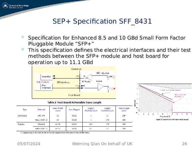
SEP Specification SFF 8431 Specification for Enhanced 8.5 and 10 GBd Small Form Factor Pluggable Module “SFP ” This specification defines the electrical interfaces and their test methods between the SFP module and host board for operation up to 11.1 GBd 05/07/2024 Weiming Qian On behalf of UK 26
SFF 8431 Defines Transmitter output Eye Mask Defines Receiver input Eye Mask 05/07/2024 Weiming Qian On behalf of UK 27
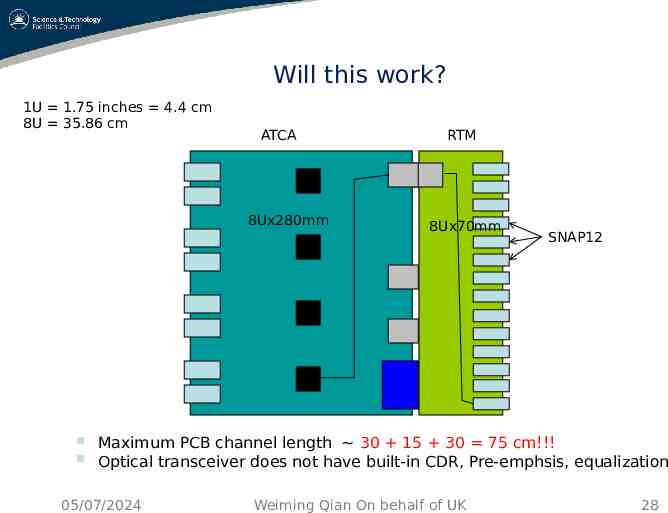
Will this work? 1U 1.75 inches 4.4 cm 8U 35.86 cm ATCA 8Ux280mm RTM 8Ux70mm SNAP12 Maximum PCB channel length 30 15 30 75 cm!!! Optical transceiver does not have built-in CDR, Pre-emphsis, equalization 05/07/2024 Weiming Qian On behalf of UK 28
Summary on high-speed PCB simulation PCB simulation becomes increasingly important as signal speed marches into Multi-Gbps range. PCB simulation is a very useful and powerful tool for Multi-Gbps PCB design provided that: Proper simulation tool Proper models Properly used Properly interpreted We have learned a lot about multi-Gbps PCB simulation tool (MentorGraphics HyperLynx SI GHz), and more importantly the underlying Signal Integrity knowledge. We are ready to integrate PCB simulation into multi-Gbps PCB design flow @RAL. We still have a lot more to learn in multi-Gbps PCB simulation. 05/07/2024 Weiming Qian On behalf of UK 29
QUIZ Given no constraints, how to make current CP/JEP working @10Gbps? What is the name of the stadium? 05/07/2024 Weiming Qian On behalf of UK 30
