Fisica dei Rivelatori di Particelle Prof.ssa M. Primavera
50 Slides5.56 MB
Fisica dei Rivelatori di Particelle Prof.ssa M. Primavera Silicon Pixel Sensors for Vertex Detectors Maria Rita Coluccia Lecce, 15 Febbraio 2007 Ciclo XIX di Dottorato in Fisica 1
Outline Silicon detector as vertex detector pn junction why silicon Si strip vs Si pixel detector Radiation Hardness Radiation damage in silicon Sensor radiation hardness Atlas and CMS silicon pixel detector Next generation of pixel detectors 2
Silicon Detector as Vertex Detector Determine position of primary interaction and secondary decay vertex o Superb position resolution o Close to interaction point o Highly segmented Radiation hardness Low mass Minimize multiple scattering o o o o Detector Readout Cooling/support Large signal Small amount of energy to create signal 3
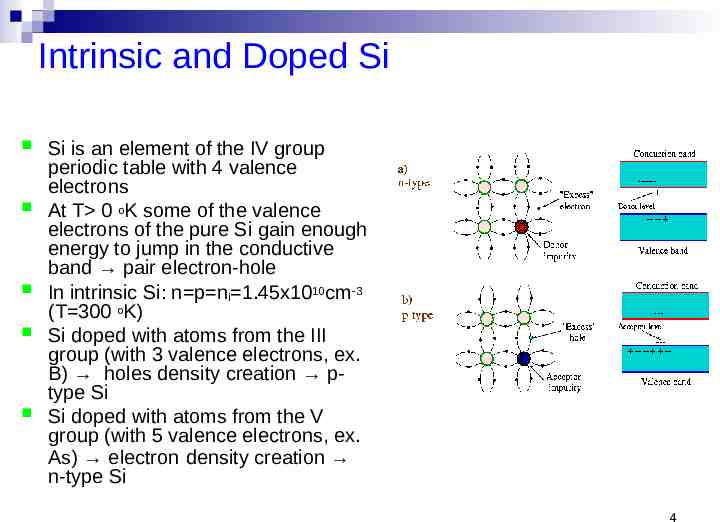
Intrinsic and Doped Si Si is an element of the IV group periodic table with 4 valence electrons At T 0 oK some of the valence electrons of the pure Si gain enough energy to jump in the conductive band pair electron-hole In intrinsic Si: n p ni 1.45x1010cm-3 (T 300 oK) Si doped with atoms from the III group (with 3 valence electrons, ex. B) holes density creation ptype Si Si doped with atoms from the V group (with 5 valence electrons, ex. As) electron density creation n-type Si 4
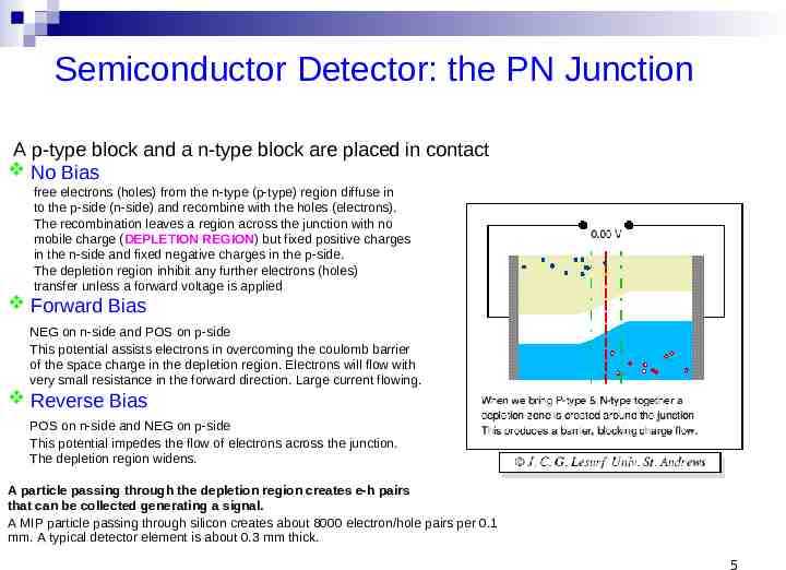
Semiconductor Detector: the PN Junction A p-type block and a n-type block are placed in contact No Bias free electrons (holes) from the n-type (p-type) region diffuse in to the p-side (n-side) and recombine with the holes (electrons). The recombination leaves a region across the junction with no mobile charge (DEPLETION REGION) but fixed positive charges in the n-side and fixed negative charges in the p-side. The depletion region inhibit any further electrons (holes) transfer unless a forward voltage is applied Forward Bias NEG on n-side and POS on p-side This potential assists electrons in overcoming the coulomb barrier of the space charge in the depletion region. Electrons will flow with very small resistance in the forward direction. Large current flowing. Reverse Bias POS on n-side and NEG on p-side This potential impedes the flow of electrons across the junction. The depletion region widens. A particle passing through the depletion region creates e-h pairs that can be collected generating a signal. A MIP particle passing through silicon creates about 8000 electron/hole pairs per 0.1 mm. A typical detector element is about 0.3 mm thick. 5
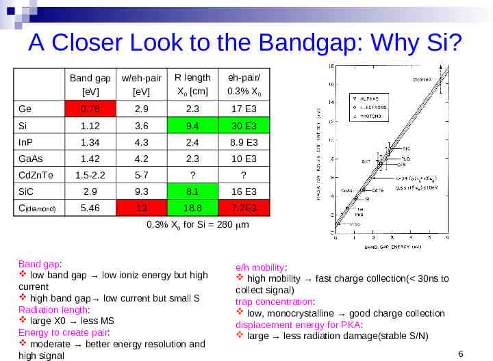
A Closer Look to the Bandgap: Why Si? Band gap [eV] w/eh-pair [eV] R length X0 [cm] eh-pair/ 0.3% X0 Ge 0.76 2.9 2.3 17 E3 Si 1.12 3.6 9.4 30 E3 InP 1.34 4.3 2.4 8.9 E3 GaAs 1.42 4.2 2.3 10 E3 1.5-2.2 5-7 ? ? SiC 2.9 9.3 8.1 16 E3 C(diamond) 5.46 13 18.8 7.2E3 CdZnTe 0.3% X0 for Si 280 m Band gap: low band gap low ioniz energy but high current high band gap low current but small S Radiation length: large X0 less MS Energy to create pair: moderate better energy resolution and high signal e/h mobility: high mobility fast charge collection( 30ns to collect signal) trap concentration: low, monocrystalline good charge collection displacement energy for PKA: large less radiation damage(stable S/N) 6
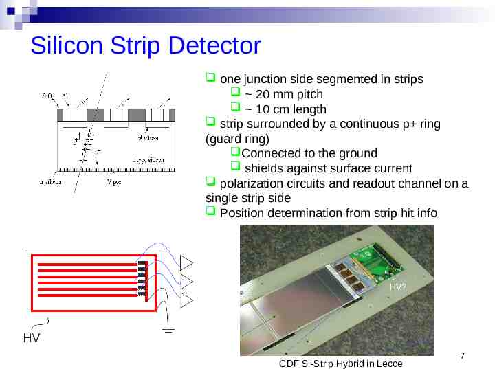
Silicon Strip Detector one junction side segmented in strips 20 mm pitch 10 cm length strip surrounded by a continuous p ring (guard ring) Connected to the ground shields against surface current polarization circuits and readout channel on a single strip side Position determination from strip hit info CDF Si-Strip Hybrid in Lecce 7
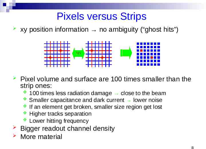
Pixels versus Strips xy position information no ambiguity (“ghost hits”) Pixel volume and surface are 100 times smaller than the strip ones: 100 times less radiation damage close to the beam Smaller capacitance and dark current lower noise If an element get broken, smaller size region get lost Higher tracks separation Lower hitting frequency Bigger readout channel density More material 8
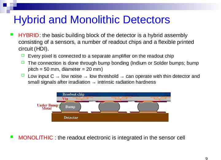
Hybrid and Monolithic Detectors HYBRID: the basic building block of the detector is a hybrid assembly consisting of a sensors, a number of readout chips and a flexible printed circuit (HDI). Every pixel is connected to a separate amplifier on the readout chip The connection is done through bump bonding (Indium or Solder bumps; bump pitch 50 mm, diameter 20 mm) Low input C low noise low threshold can operate with thin detector and small signals after irradiation intrinsic radiation hardness MONOLITHIC : the readout electronic is integrated in the sensor cell 9
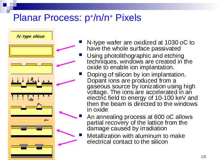
Planar Process: p /n/n Pixels N-type wafer are oxidized at 1030 oC to have the whole surface passivated Using photolithographic and etching techniques, windows are created in the oxide to enable ion implantation. Doping of silicon by ion implantation. Dopant ions are produced from a gaseous source by ionization using high voltage. The ions are accelerated in an electric field to energy of 10-100 keV and then the beam is directed to the windows in oxide An annealing process at 600 oC allows partial recovery of the lattice from the damage caused by irradiation Metallization with aluminum to make electrical contact to the silicon 10
Important Silicon Pixel Characteristics Leakage Current: thermal current of the minority carriers (depends also on light exposure) Ileak needs to be less than 100 nA @ Vdep at 20 oC Need to have high breakdown voltage (Ileak increase steeply and is bigger than 1 mA @ Vbreak ) Depletion Voltage: voltage needed to have the semiconductor bulk completely depleted of free carriers a) Important to check the integrity of the sensor before the bump-bonding to the electronics Important to predict a “Test Structure” in the sensor design Standard techniques are adopted: I-V, C-V, V-V curves b) c) 11
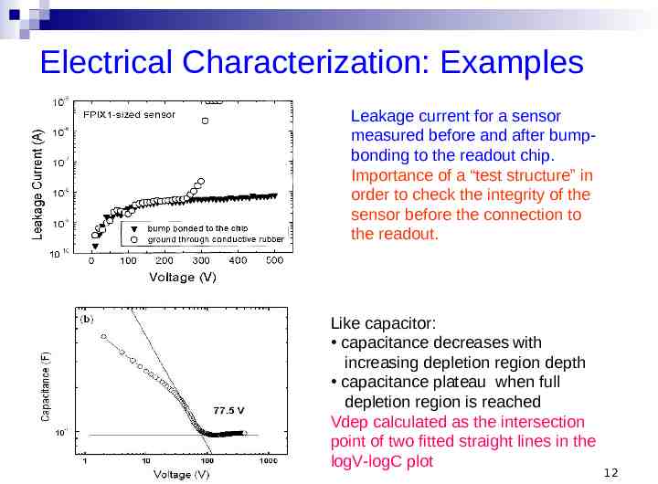
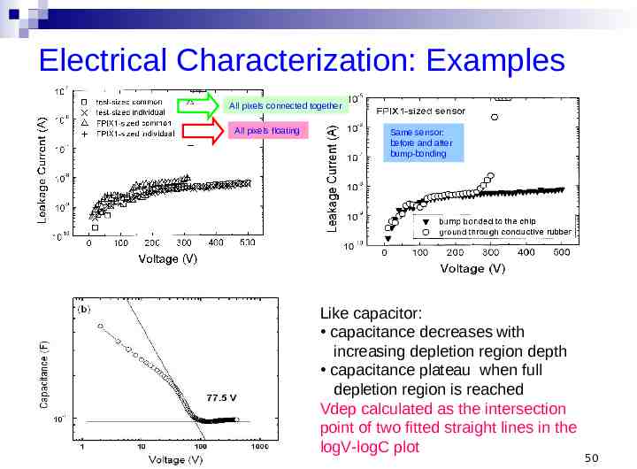
Electrical Characterization: Examples Leakage current for a sensor measured before and after bumpbonding to the readout chip. Importance of a “test structure” in order to check the integrity of the sensor before the connection to the readout. Like capacitor: capacitance decreases with increasing depletion region depth capacitance plateau when full depletion region is reached Vdep calculated as the intersection point of two fitted straight lines in the logV-logC plot 12
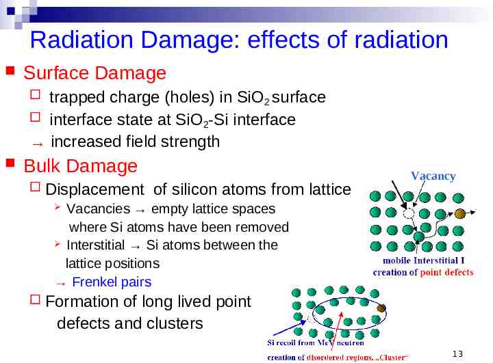
Radiation Damage: effects of radiation Surface Damage trapped charge (holes) in SiO2 surface interface state at SiO2-Si interface increased field strength Bulk Damage Displacement of silicon atoms from lattice Vacancy Vacancies empty lattice spaces where Si atoms have been removed Interstitial Si atoms between the lattice positions Frenkel pairs Formation of long lived point defects and clusters 13
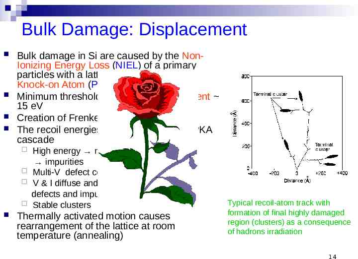
Bulk Damage: Displacement Bulk damage in Si are caused by the NonIonizing Energy Loss (NIEL) of a primary particles with a lattice Si atom Primary Knock-on Atom (PKA) Minimum threshold energy for displacement 15 eV Creation of Frenkel pairs (V-I) The recoil energies of PKAs can create PKA cascade High energy nuclear reaction impurities Multi-V defect complexes V & I diffuse and react with defects and impurities Stable clusters Thermally activated motion causes rearrangement of the lattice at room temperature (annealing) Typical recoil-atom track with formation of final highly damaged region (clusters) as a consequence of hadrons irradiation 14
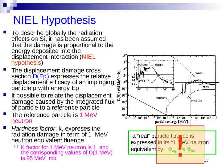
NIEL Hypothesis To describe globally the radiation effects on Si, it has been assumed that the damage is proportional to the energy deposited into the displacement interaction (NIEL hypothesis) The displacement damage cross section D(Ep) expresses the relative displacement efficacy of an impinging particle p with energy Ep It possible to relate the displacement damage caused by the integrated flux of particle to a reference particle The reference particle is 1 MeV neutron Hardness factor, k, expreses the radiation damage in term of 1 MeV neutron equivalent fluence K factor for 1 MeV neutron is 1 and the corrisponding values of D(1 MeV) is 95 MeV mb ! a “real” particle fluence is expressed in its “1 MeV neutron” equivalent by: eq k tot 15
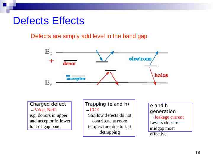
Defects Effects Defects are simply add level in the band gap Charged defect Vdep, Neff e.g. donors in upper and acceptor in lower half of gap band Trapping (e and h) CCE Shallow defects do not contribute at room temperature due to fast detrapping e and h generation leakage current Levels close to midgap most effective 16
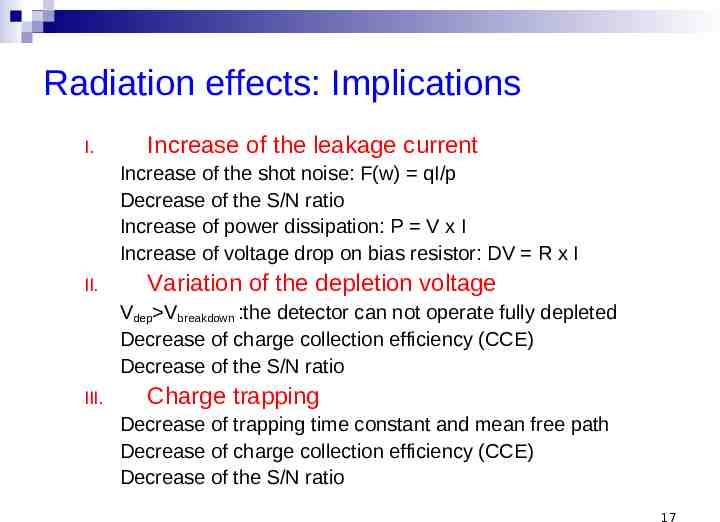
Radiation effects: Implications I. Increase of the leakage current Increase of the shot noise: F(w) qI/p Decrease of the S/N ratio Increase of power dissipation: P V x I Increase of voltage drop on bias resistor: DV R x I II. Variation of the depletion voltage Vdep Vbreakdown :the detector can not operate fully depleted Decrease of charge collection efficiency (CCE) Decrease of the S/N ratio III. Charge trapping Decrease of trapping time constant and mean free path Decrease of charge collection efficiency (CCE) Decrease of the S/N ratio 17
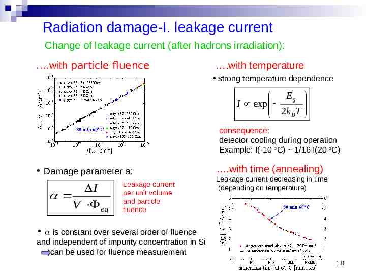
Radiation damage-I. leakage current Change of leakage current (after hadrons irradiation): .with particle fluence .with temperature strong temperature dependence Eg I exp 2k B T consequence: detector cooling during operation Example: I(-10 oC) 1/16 I(20 oC) Damage parameter a: I V eq Leakage current per unit volume and particle fluence .with time (annealing) Leakage current decreasing in time (depending on temperature) is constant over several order of fluence and independent of impurity concentration in Si can be used for fluence measurement 18
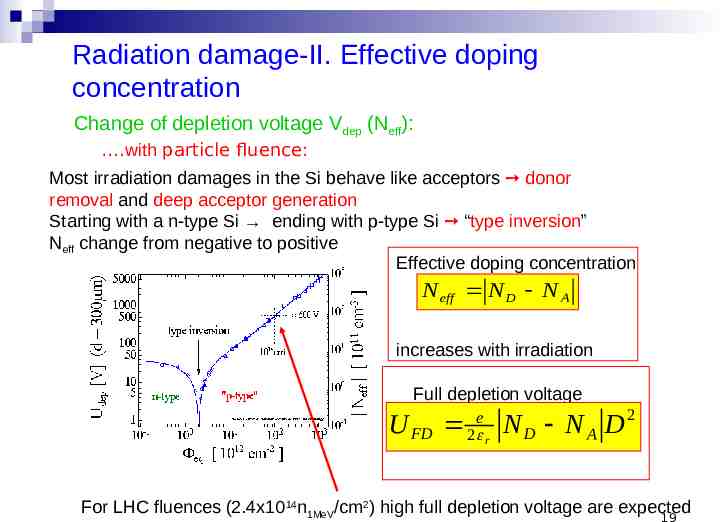
Radiation damage-II. Effective doping concentration Change of depletion voltage Vdep (Neff): .with particle fluence: Most irradiation damages in the Si behave like acceptors donor removal and deep acceptor generation Starting with a n-type Si ending with p-type Si “type inversion” Neff change from negative to positive Effective doping concentration N eff N D N A increases with irradiation Full depletion voltage U FD 2e r N D N A D 2 For LHC fluences (2.4x10¹⁴n1MeV/cm2) high full depletion voltage are expected 19
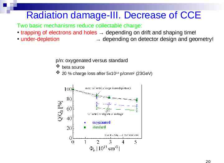
Radiation damage-III. Decrease of CCE Two basic mechanisms reduce collectable charge: trapping of electrons and holes depending on drift and shaping time! under-depletion depending on detector design and geometry! p/n: oxygenated versus standard beta source 20 % charge loss after 5x10¹⁴ p/cmm2 (23GeV) 20
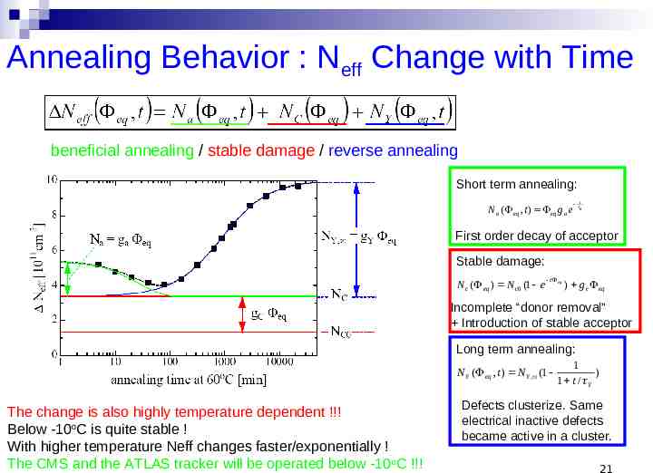
Annealing Behavior : Neff Change with Time beneficial annealing / stable damage / reverse annealing Short term annealing: N a ( eq , t ) eq g a e t a N a ( eq , t ) eq g a e t a First order decay of acceptor Stable damage: N c ( eq ) N c 0 (1 e c eq ) g c eq Incomplete “donor removal” Introduction of stable acceptor N a ( eq , t ) eq g a e t a Long term annealing: N Y ( eq , t ) N Y , (1 The change is also highly temperature dependent !!! Below -10oC is quite stable ! With higher temperature Neff changes faster/exponentially ! The CMS and the ATLAS tracker will be operated below -10 oC !!! 1 ) 1 t / Y Defects clusterize. Same electrical inactive defects became active in a cluster. 21
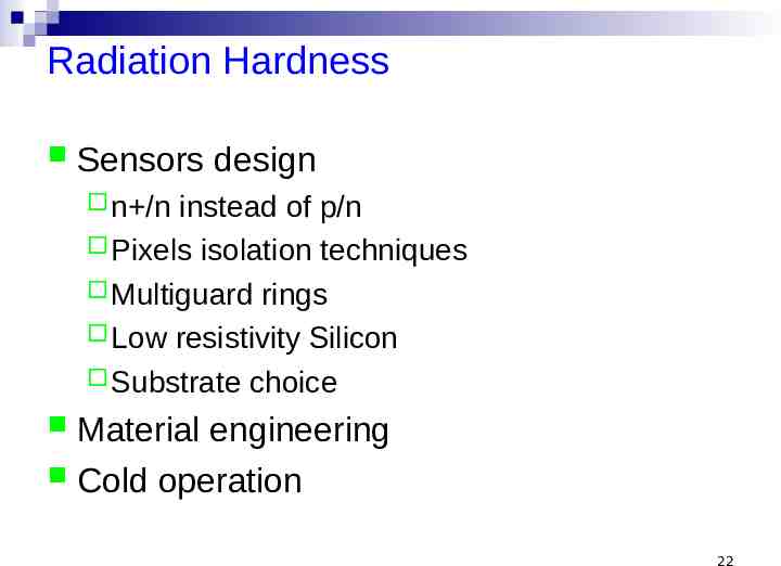
Radiation Hardness Sensors design n /n instead of p/n Pixels isolation techniques Multiguard rings Low resistivity Silicon Substrate choice Material engineering Cold operation 22
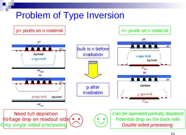
Problem of Type Inversion p pixels on n material n pixels on n material bulk is n before irradiation p after irradiation Need full depletion Voltage drop on readout side Only single sided processing Can be operated partially depleted Potential drop on the back side Double sided processing 23
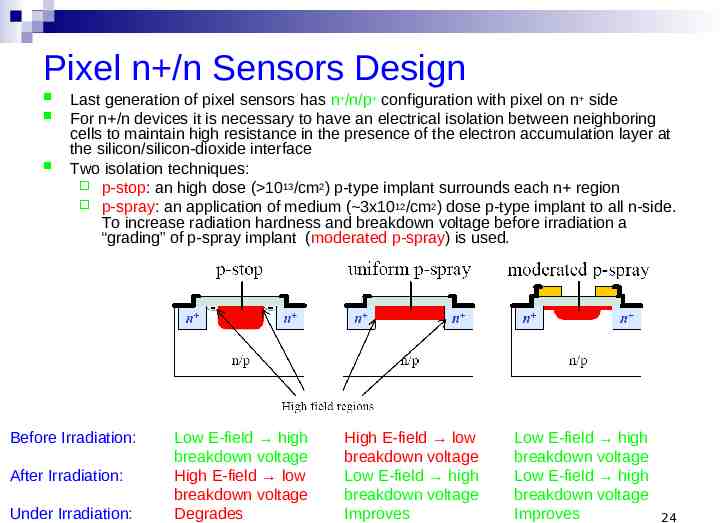
Pixel n /n Sensors Design Last generation of pixel sensors has n /n/p configuration with pixel on n side For n /n devices it is necessary to have an electrical isolation between neighboring cells to maintain high resistance in the presence of the electron accumulation layer at the silicon/silicon-dioxide interface Two isolation techniques: p-stop: an high dose ( 1013/cm2) p-type implant surrounds each n region p-spray: an application of medium ( 3x10¹²/cm2) dose p-type implant to all n-side. To increase radiation hardness and breakdown voltage before irradiation a “grading” of p-spray implant (moderated p-spray) is used. Before Irradiation: After Irradiation: Under Irradiation: Low E-field high breakdown voltage High E-field low breakdown voltage Degrades High E-field low breakdown voltage Low E-field high breakdown voltage Improves Low E-field high breakdown voltage Low E-field high breakdown voltage Improves 24
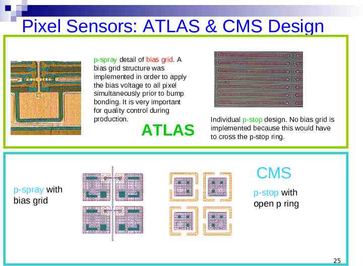
Pixel Sensors: ATLAS & CMS Design p-spray detail of bias grid. A bias grid structure was implemented in order to apply the bias voltage to all pixel simultaneously prior to bump bonding. It is very important for quality control during production. ATLAS Individual p-stop design. No bias grid is implemented because this would have to cross the p-stop ring. CMS p-spray with bias grid p-stop with open p ring 25
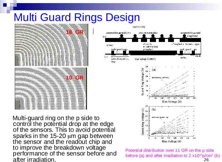
Multi Guard Rings Design 18 GR 10 GR Multi-guard ring on the p side to control the potential drop at the edge of the sensors. This to avoid potential sparks in the 15-20 m gap between the sensor and the readout chip and to improve the breakdown voltage performance of the sensor before and after irradiation. Potential distribution over 11 GR on the p side before (a) and after irradiation to 2 x10 14p/cm2 (b) 26
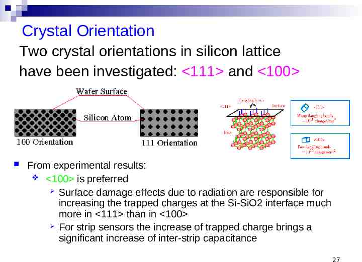
Crystal Orientation Two crystal orientations in silicon lattice have been investigated: 111 and 100 From experimental results: 100 is preferred Surface damage effects due to radiation are responsible for increasing the trapped charges at the Si-SiO2 interface much more in 111 than in 100 For strip sensors the increase of trapped charge brings a significant increase of inter-strip capacitance 27
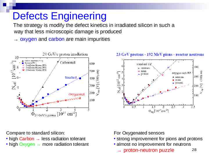
Defects Engineering The strategy is modify the defect kinetics in irradiated silicon in such a way that less microscopic damage is produced oxygen and carbon are main impurities Compare to standard silicon: high Carbon less radiation tolerant high Oxygen more radiation tolerant For Oxygenated sensors strong improvement for pions and protons almost no improvement for neutrons proton-neutron puzzle 28
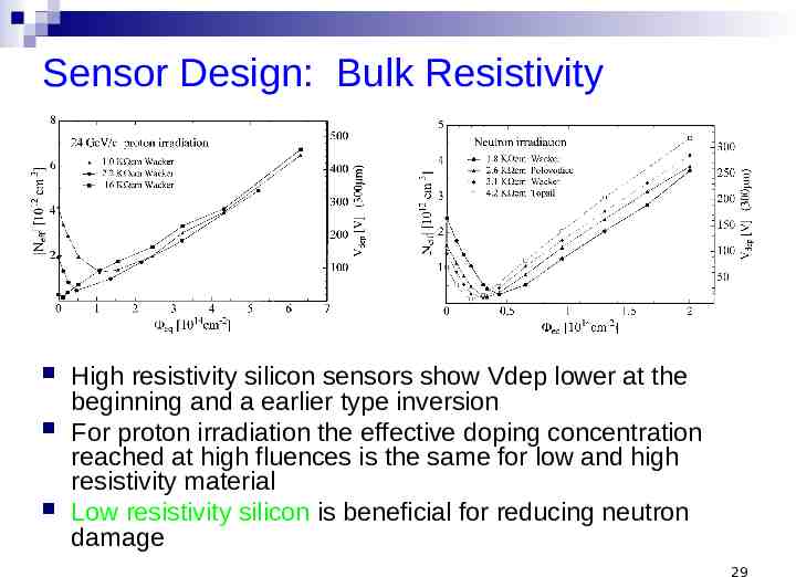
Sensor Design: Bulk Resistivity High resistivity silicon sensors show Vdep lower at the beginning and a earlier type inversion For proton irradiation the effective doping concentration reached at high fluences is the same for low and high resistivity material Low resistivity silicon is beneficial for reducing neutron damage 29
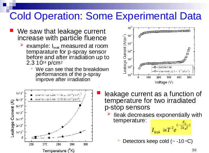
Cold Operation: Some Experimental Data We saw that leakage current increase with particle fluence example: Ileak measured at room temparature for p-spray sensor before and after irradiation up to 2.3 1014 p/cm2 We can see that the breakdown performances of the p-spray improve after irradiation leakage current as a function of temperature for two irradiated p-stop sensors Ileak decreases exponentially with temperature: Eg 2 I leak T e ( 2 k BT ) Detectors keep cold ( -10 oC) 30
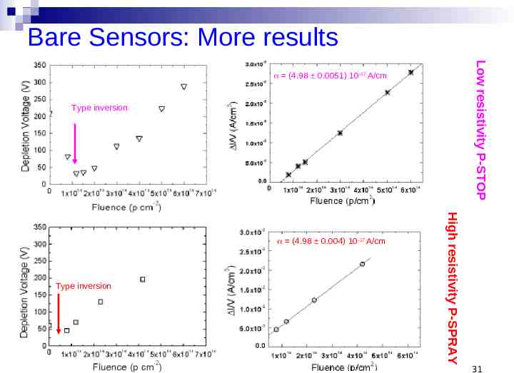
Bare Sensors: More results Low resistivity P-STOP (4.98 0.0051) 10-17 A/cm Type inversion Type inversion High resistivity P-SPRAY (4.98 0.004) 10-17 A/cm 31
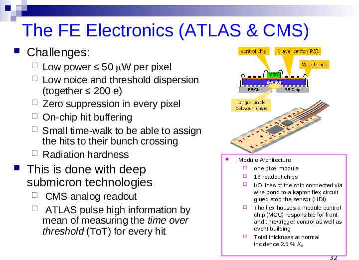
The FE Electronics (ATLAS & CMS) Challenges: Low power 50 W per pixel Low noice and threshold dispersion (together 200 e) Zero suppression in every pixel On-chip hit buffering Small time-walk to be able to assign the hits to their bunch crossing Radiation hardness This is done with deep submicron technologies CMS analog readout ATLAS pulse high information by mean of measuring the time over threshold (ToT) for every hit Module Architecture one pixel module 16 readout chips I/O lines of the chip connected via wire bond to a kapton flex circuit glued atop the sensor (HDI) The flex houses a module control chip (MCC) responsible for front and time/trigger control as well as event building Total thickness at normal incidence 2.5 % X0 32
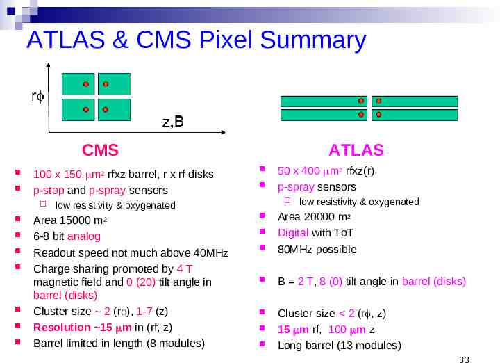
ATLAS & CMS Pixel Summary CMS 100 x 150 m2 rfхz barrel, r х rf disks p-stop and p-spray sensors ATLAS low resistivity & oxygenated Area 15000 m2 6-8 bit analog Readout speed not much above 40MHz Charge sharing promoted by 4 T magnetic field and 0 (20) tilt angle in barrel (disks) Cluster size 2 (r ), 1-7 (z) Resolution 15 m in (rf, z) Barrel limited in length (8 modules) 50 x 400 m2 rfхz(r) p-spray sensors low resistivity & oxygenated Area 20000 m2 Digital with ToT 80MHz possible B 2 T, 8 (0) tilt angle in barrel (disks) Cluster size 2 (r , z) 15 m rf, 100 m z Long barrel (13 modules) 33
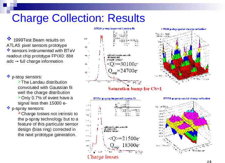
Charge Collection: Results 1999Test Beam results on ATLAS pixel sensors prototype sensors instrumented with BTeV readout chip prototype FPIX0: 8bit adc full charge information p-stop sensors: The Landau distribution convoluted with Gaussian fit well the charge distribution Only 0.7% of event have a signal less then 15000 e p-spray sensors: Charge losses not intrinsic to the p-spray technology but to a feature of this particular sensor design (bias ring) corrected in the next prototype generation. 34
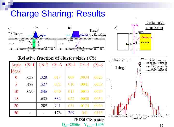
Charge Sharing: Results For all angles there is a small fraction of cluster with multiplicity bigger respect to the one expected from diffusion and geometry delta rays They can influence also the most probable CS, in fact the residual distributions can present non-gaussian tails!!! 35
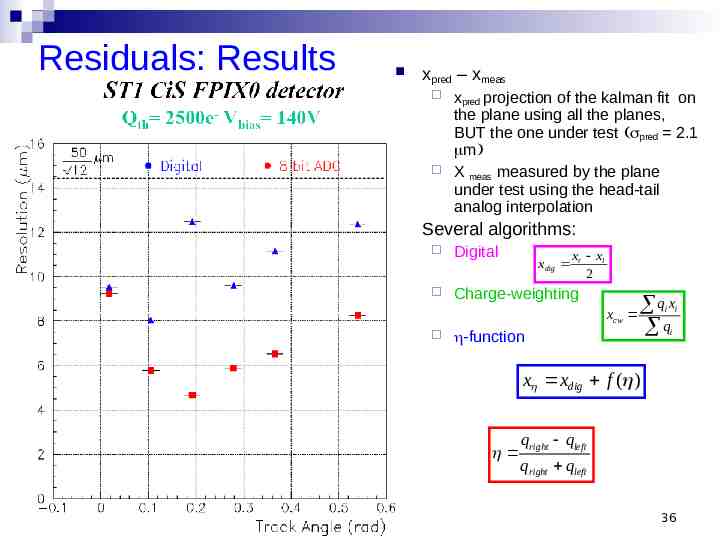
Residuals: Results xpred – xmeas xpred projection of the kalman fit on the plane using all the planes, BUT the one under test pred 2.1 m X meas measured by the plane under test using the head-tail analog interpolation Several algorithms: Digital Charge-weighting xdig xr xl 2 xcw -function q x q i i i x xdig f ( ) qright qleft qright qleft 36
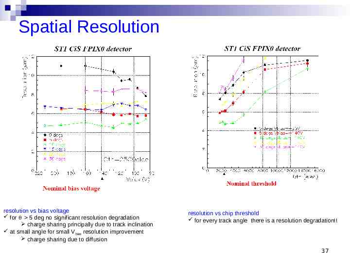
Spatial Resolution resolution vs bias voltage for 5 deg no significant resolution degradation charge sharing principally due to track inclination at small angle for small Vbias resolution improvement charge sharing due to diffusion resolution vs chip threshold for every track angle there is a resolution degradation!! 37
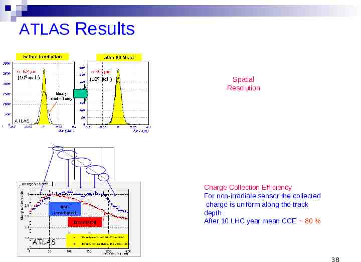
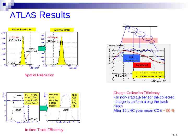
ATLAS Results Spatial Resolution Charge Collection Efficiency For non-irradiate sensor the collected charge is uniform along the track depth After 10 LHC year mean CCE 80 % 38
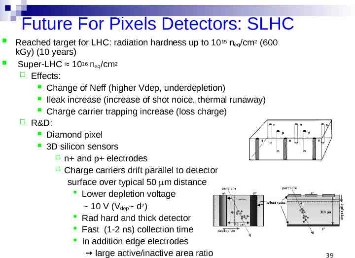
Future For Pixels Detectors: SLHC Reached target for LHC: radiation hardness up to 1015 neq/cm2 (600 kGy) (10 years) Super-LHC 1016 neq/cm2 Effects: Change of Neff (higher Vdep, underdepletion) Ileak increase (increase of shot noice, thermal runaway) Charge carrier trapping increase (loss charge) R&D: Diamond pixel 3D silicon sensors n and p electrodes Charge carriers drift parallel to detector surface over typical 50 m distance Lower depletion voltage 10 V (Vdep d2) Rad hard and thick detector Fast (1-2 ns) collection time In addition edge electrodes large active/inactive area ratio 39
Future For Pixels Detectors: ILC Challenges due to very intense beamstrahlung of narrowly focused electron beams close to the interaction region: Very low ( 1 % X0) material per detector layer Small pixel size ( 20 m x 20 m) High rate capability (80 hits/mm2/ms) High readout speed with typical line rates of several 10 MHz and a 40 s frame readout time are necessary R&D on monolithic pixel detectors amplifying and logic circuit as well as radiation detecting sensor are one entity CMOS active pixel MAPS DEPFET pixel 40
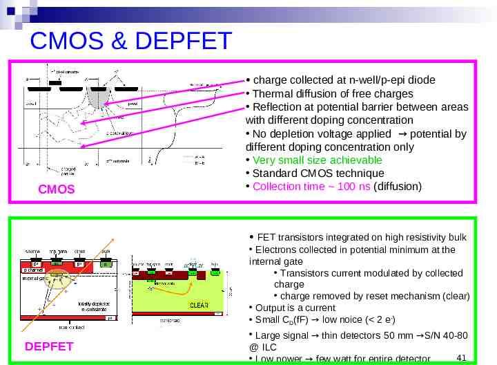
CMOS & DEPFET charge collected at n-well/p-epi diode CMOS Thermal diffusion of free charges Reflection at potential barrier between areas with different doping concentration No depletion voltage applied potential by different doping concentration only Very small size achievable Standard CMOS technique Collection time 100 ns (diffusion) FET transistors integrated on high resistivity bulk DEPFET Electrons collected in potential minimum at the internal gate Transistors current modulated by collected charge charge removed by reset mechanism (clear) Output is a current Small CD(fF) low noice ( 2 e-) Large signal thin detectors 50 mm S/N 40-80 @ ILC 41 Low power few watt for entire detector
AT THE END . THE END !!!!! 42
Charge Signal in Silicon Very important for better understanding the sensor behavior and for valuating the impact point of the particles on detectors (residuals) Particles traversing the sensors release a small energy fraction This energy release presents fluctuations These fluctuations follow the Landau distribution (theory based on Rutherford scattering) Theory improved by Vavilov that takes into account the spin of the incident particles and the fact that there is a limit to the quantity of energy that a heavy particle (es. p, K, p) can transfer to an electron in the bulk From the Landau distribution The peak gives the most probable energy released (Emp) The is a tail for high energy due to few collisions with a considerable amount of energy transferred (d rays) Full Width Half Maximum FWHM that is 20% of Emp Landau-Vavilov theory need correction because we need to consider that the electrons in the bulk material are not free Emp from theory is in good agreement with data but the distribution is much more large this effect is as bigger as lower is the sensor thickness Shulek found out that the energy loss fluctuation in a small bulk can be described by a Landau distribution convoluted with a Gaussian f ( E ) NdE ' e ( E E ') 2 2 g2 2 g2 ( E EMP 0 ) 43
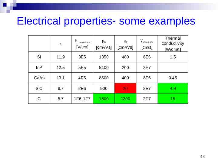
Electrical properties- some examples E break-down e h vsaturation [V/cm] [cm2/Vs] [cm2/Vs] [cm/s] Thermal conductivity [W/cmK] Si 11.9 3E5 1350 480 8E6 1.5 InP 12.5 5E5 5400 200 3E7 GaAs 13.1 4E5 8500 400 8E6 0.45 SiC 9.7 2E6 900 20 2E7 4.9 C 5.7 1E6-1E7 1800 1200 2E7 15 44
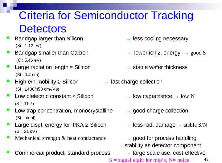
Criteria for Semiconductor Tracking Detectors Bandgap larger than Silicon less cooling necessary (Si : 1.12 eV) Bandgap smaller than Carbon lower ioniz. energy good S (C : 5.46 eV) Large radiation length Silicon stable wafer thickness (Si : 9.4 cm) High e/h-mobility Silicon fast charge collection (Si : 1400/450 cm2/Vs) Low dielectric constant Silicon low capacitance low N (Si : 11.7) Low trap concentration, monocrystalline good charge collection (Si : ideal) Large displ. energy for PKA Silicon less rad. damage stable S/N (Si : 21 eV) good for process handling stability as detector component Commercial product, standard process large scale use, cost effective 45 S signal eight for mip’s, N noice Mechanical strength & heat conductance
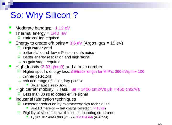
So: Why Silicon ? Moderate bandgap 1.12 eV Thermal energy 1/40 eV Little cooling required Energy to create e/h pairs 3.6 eV (Argon gas 15 eV) High carrier yield better stats and lower Poisson stats noise Better energy resolution and high signal no gain stage required High density (2.33 g/cm3) and atomic number Higher specific energy loss: ΔE/track length for MIP’s: 390 eV/μm 100 thinner detectors reduced range of secondary particle High carrier mobility fast!! μe 1450 cm2/Vs μh 450 cm2/Vs Better spatial resolution Less than 30 ns to collect entire signal Industrial fabrication techniques Detector production by microelectronics techniques Small dimension fast charge collection ( 10 ns) Rigidity of silicon allows thin self supporting structures Typical thickness 300 μm 3.2 104 e-h (average) 46
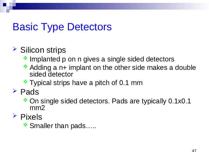
Basic Type Detectors Silicon strips Implanted p on n gives a single sided detectors Adding a n implant on the other side makes a double sided detector Typical strips have a pitch of 0.1 mm Pads On single sided detectors. Pads are typically 0.1x0.1 mm2 Pixels Smaller than pads . 47
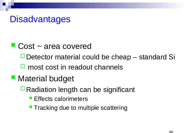
Disadvantages Cost area covered Detector material could be cheap – standard Si most cost in readout channels Material budget Radiation length can be significant Effects calorimeters Tracking due to multiple scattering 48
ATLAS Results Spatial Resolution Charge Collection Efficiency For non-irradiate sensor the collected charge is uniform along the track depth After 10 LHC year mean CCE 80 % In-time Track Efficiency 49
Electrical Characterization: Examples All pixels connected together All pixels floating Same sensor: before and after bump-bonding Like capacitor: capacitance decreases with increasing depletion region depth capacitance plateau when full depletion region is reached Vdep calculated as the intersection point of two fitted straight lines in the logV-logC plot 50
